15i/150i - Model B Connection manual (Hardware) Page 101
Connection manual (Hardware)
B–63783EN/01
6. CONNECTION OF I/O UNITS TO
MACHINE INTERFACE
89
7
X
Module internal address
Yn
Yn+1
X
6
X
X
5
X
X
4
X
X
3
X
X
2
X
X
1
X
CHB
0
X
CHA
Specifying a pair of values listed below for CHA and CHB causes the
corresponding channel to be selected, thus enabling the A–D conversion
and selection data for the channel to be read as DI data. Letter X in the
above table indicates a bit not in use. It can be either 0 or 1.
CHB CHA Channel to be selected
0 0 Channel 1
0 1 Channel 2
1 0 Channel 3
1 1 Channel 4
(About the addresses)
The first address for X (DI) of the basic modules containing an analog
input module must be even–numbered. With this assignment, the digital
output address of the analog input module is determined based on the
space where it is mounted, as listed below.
D If the analog input module is mounted in the space for expansion
module 1 (m is the top address assigned)
76543210
Undefined
D07 D06 D05 D04 D03 D02 D01 D00
0 0 CHB CHA D11 D10 D09 D08
Module internal address
Xm+3 (odd address)
Xm+4 (even address)
Xm+5 (odd address)
D If the analog input module is mounted in the space for expansion
module 2 (m is the first assigned address)
76543210
D07 D06 D05 D04 D03 D02 D01 D00
0 0 CHB CHA D11 D10 D09 D08
Undefined
Module internal address
Xm+6 (odd address)
Xm+7 (even address)
Xm+8 (odd address)
Contents Summary of 15i/150i - Model B Connection manual (Hardware)
- Page 1CONNECTION MANUAL (HARDWARE) B-63783EN/01�
- Page 2• No part of this manual may be reproduced in any form. • All specifications and designs are subject to change without notice. The export of this product is subject to the authorization of the government of the country from where the product is exported. In this manual we have tried as much as possi
- Page 3B–63783EN/01 DEFINITION OF WARNING, CAUTION, AND NOTE DEFINITION OF WARNING, CAUTION, AND NOTE This manual includes safety precautions for protecting the user and preventing damage to the machine. Precautions are classified into Warning and Caution according to their bearing on safety. Also, supplem
- Page 4
- Page 5B–63783EN/01 Table of Contents DEFINITION OF WARNING, CAUTION, AND NOTE . . . . . . . . . . . . . . . . . . . . . . . . . . s–1 1. GENERAL . . . . . . . . . . . . . . . . . . . . . . . . . . . . . . . . . . . . . . . . . . . . . . . . . . . . . . . . . . . . 1 2. CONFIGURATION . . . . . . . . . . .
- Page 6Table of Contents B–63783EN/01 6.2.1 Connection of FANUC I/O Link by Electric Cable . . . . . . . . . . . . . . . . . . . . . . . . . . . . . . . . . . . . . . . . 65 6.2.2 Connection of FANUC I/O Link Optical Fiber Cable . . . . . . . . . . . . . . . . . . . . . . . . . . . . . . . . . . . . . . 66
- Page 7B–63783EN/01 Table of Contents 6.7 CONNECTION OF MACHINE OPERATOR’S PANEL INTERFACE UNIT . . . . . . . . . . . . . . . . . 152 6.7.1 Function Overview . . . . . . . . . . . . . . . . . . . . . . . . . . . . . . . . . . . . . . . . . . . . . . . . . . . . . . . . . . . . . . . . 152 6.7.2 System Conf
- Page 8Table of Contents B–63783EN/01 6.12.6.2 Main panel A/B/A1/B1 specification . . . . . . . . . . . . . . . . . . . . . . . . . . . . . . . . . . . . . . . . . . . . 255 6.12.6.3 Sub panel A/B/B1/C/C1 specification . . . . . . . . . . . . . . . . . . . . . . . . . . . . . . . . . . . . . . . . . . . 25
- Page 9B–63783EN/01 Table of Contents 7.8.2 Serial Communication Board A2 (RS–422) . . . . . . . . . . . . . . . . . . . . . . . . . . . . . . . . . . . . . . . . . . . . . 314 8. CONNECTION TO OTHER NETWORKS . . . . . . . . . . . . . . . . . . . . . . . . . . . . . . . . . . 316 9. HIGH–SPEED SERIAL BUS (
- Page 10Table of Contents B–63783EN/01 10.8.2 Method of Mounting PCI Extension Board . . . . . . . . . . . . . . . . . . . . . . . . . . . . . . . . . . . . . . . . . . . . . 356 10.8.3 Method of Mounting PCI Extension Board . . . . . . . . . . . . . . . . . . . . . . . . . . . . . . . . . . . . . . . . . .
- Page 11B–63783EN/01 Table of Contents H.3.1 Pin Assignment . . . . . . . . . . . . . . . . . . . . . . . . . . . . . . . . . . . . . . . . . . . . . . . . . . . . . . . . . . . . . . . . . . 485 H.3.2 Connection of 24VDC Power Supply and Signals . . . . . . . . . . . . . . . . . . . . . . . . . . . . . . .
- Page 12
- Page 13B–63783EN/01 1. GENERAL 1 GENERAL Contents of this manual This manual describes the electrical and structural specifications required for connecting the CNC control units, FANUC Series 15i/150i, with a machine tool, and covers the equipment shown in the configuration diagram in Chapter 2. When using
- Page 141. GENERAL B–63783EN/01 9. HIGH–SPEED SERIAL BUS (HSSB) This chapter describes the high–speed serial bus (HSSB), which enables transfer of data between the CNC and the personal computer. 10.CNC DISPLAY UNIT WITH PC FUNCTIONS This chapter describes how to connect the CNC to the CNC display unit with
- Page 15B–63783EN/01 1. GENERAL Related manuals The table below lists manuals related to FANUC Series 15i/150i–MODEL B. In the table, this manual is marked with an asterisk(*). Table 1 Related manuals Specification Manual name number DESCRIPTIONS B–63782EN CONNECTION MANUAL (Hardware) B–63783EN * CONNECTION
- Page 162. CONFIGURATION B–63783EN/01 2 CONFIGURATION The following figure shows the configuration of the electrical system of the machine tool with which this control is used. This manual describes how to connect the units illustrated in this diagram. The machine tool body, machine operator’s panel, power
- Page 17B–63783EN/01 2. CONFIGURATION Machine tool magnetics cabinet I/O unit LCD unit Memory card Heat exchanger MDI unit I/O unit CNC Manual pulse generator Operator’s Machine panel I/O unit operator’s panel Wiring panel Power mag- netics cabinet Sensors I/O unit control circuit Servo Servo amplifier moto
- Page 183. INSTALLATION B–63783EN/01 3 INSTALLATION 6
- Page 19B–63783EN/01 3. INSTALLATION 3.1 ENVIRONMENTAL REQUIREMENTS OUTSIDE THE CABINET 3.1.1 The peripheral units and the control unit have been designed on the assumption that they are housed in closed cabinets. In this manual Environmental “cabinet” refers to the following: Conditions Around the D Cabine
- Page 203. INSTALLATION B–63783EN/01 3.1.2 Installation Conditions Operating: 0°C to 55°C for the CNC and Servo (no hard disk drive used) Unit Inside the Cabinet Ambient temperature Operating: 5°C to 50°C (hard disk drive used) Storage and transportation: –20°C to 60°C 95% or less (relative) with no condens
- Page 21B–63783EN/01 3. INSTALLATION 3.2 The power requirement of the CNC control unit is calculated as the sum of the power required by the control and servo sections. POWER REQUIREMENTS The control section power requirement includes the power required for control, the LCD, I/O units, the operator panel in
- Page 223. INSTALLATION B–63783EN/01 3.3 When a cabinet is designed, it must satisfy the environmental conditions described in Section 3.1. In addition, the magnetic interference on the DESIGN AND screen, noise resistance, and maintenance requirements must be INSTALLATION considered. The cabinet design must
- Page 23B–63783EN/01 3. INSTALLATION Top Connector panel I/O module or I/O base unit (No screws or protrusions shall extend from the bottom of this unit.) Bottom D If the CNC unit is installed at an altitude of over 1,000 m, an upper limit is placed on the ambient temperature (one of the environmental condi
- Page 243. INSTALLATION B–63783EN/01 3.4 When a cabinet or a pendant box, which houses a display and an operator’s panel, is designed, it must satisfy following conditions to prevent from PROTECTION OF the entry of airborne dust, coolant, and organic solvent. PARTS INSIDE A (1) A cabinet or a pendant box mu
- Page 25B–63783EN/01 3. INSTALLATION 3.5 The purpose of the thermal design of the cabinet is to limit the difference in temperature between the air in the cabinet and the outside air to 10°C THERMAL DESIGN or less when the temperature in the cabinet increases. OF THE CABINET The internal air temperature of
- Page 263. INSTALLATION B–63783EN/01 3.5.3 Calorific Value of Each Unit Product name Calorific value Remarks Control unit Basic unit (2 slots) 64W Basic unit (4 slots) 68W Main CPU board 38W Additional axis board 10W HSSB board 4W Data server board A1 6W Data server board A2 6.3W Including the 0.3 W of the
- Page 27B–63783EN/01 3. INSTALLATION Product name Calorific value Remarks I/O unit model B BIF04A1 1.6W AIF02C 1.2W BID16A1, BID16B1 1.5W + 0.23 × Number of ON inputs BID16P1, BID16Q1 0.6W + 0.23 × Number of ON inputs BOA12A1 0.9W + (0.09 + 1.1 × IL2) x Number of ON outputs BOD16A1 1.0W + (0.13 + 0.3 × IL2)
- Page 283. INSTALLATION B–63783EN/01 3.6 The CNC has been steadily reduced in size using surface–mount and custom LSI technologies for electronic components. The CNC also is ACTION AGAINST designed to be protected from external noise. However, it is difficult to NOISE measure the level and frequency of nois
- Page 29B–63783EN/01 3. INSTALLATION NOTE 1 The groups must be 10 cm or more apart from one another when binding the cables in each group. 2 The electromagnetic shield refers to shielding between groups with grounded steel plates. 3.6.2 The CNC machine tool has three grounding systems: Grounding D Grounding
- Page 303. INSTALLATION B–63783EN/01 Notes on wiring for the D The ground resistance of the protective earth (PE) system must be grounding systems 100 Ω or less (as per class–D grounding). D The connection cable for the protective earth (PE) system must be so large in cross section that the accidental curre
- Page 31B–63783EN/01 3. INSTALLATION (b) Display unit (rear view) Cover PCB CP1 COP20 B A M4 stud for earth connection (c) MDI unit (rear view) CK2 CK1 M4 stud for earth connection 19
- Page 323. INSTALLATION B–63783EN/01 (d) Connection units 1, 2 M4 screw (e) Operator’s panel connection unit Install an installation plate. (f) I/O unit model A Connect the grounding terminals of ABU05A, ABU05B, ABU10A and ABU10B. ABU05A, ABU10A ABU05B, ABU10B M4 screw terminal for grounding SG terminal (M3
- Page 33B–63783EN/01 3. INSTALLATION (g) Hard disk unit Control unit Grounding terminal for signals Printed circuit board Hard disk unit Grounding terminal for signals M3 terminal block (FG1) Grounding cable Grounding cable Grounding plate of the cabinet NOTE Connect the grounding cable of the hard disk uni
- Page 343. INSTALLATION B–63783EN/01 3.6.4 AC/DC solenoids and relays are used in the power magnetics cabinet. Noise Suppresser A high pulse voltage is caused by coil inductance when these devices are turned on or off. This pulse voltage induced through the cable causes the electronic circuits to be disturb
- Page 35B–63783EN/01 3. INSTALLATION 3.6.5 The CNC cables that require shielding should be clamped by the method Cable Clamp and shown below. This cable clamp treatment is for both cable support and proper grounding of the shield. To ensure stable CNC system operation, Shield Processing follow this cable ca
- Page 363. INSTALLATION B–63783EN/01 ÇÇ Machine side installation ÇÇ board ÇÇ Control unit ÇÇ ÇÇ ÇÇ ÇÇ ÇÇ ÇÇ ÇÇ ÇÇ Ground plate ÇÇ ÇÇ ÇÇ Metal fittings ÇÇ ÇÇ for clamp Shield cover Fig. 3.6.5 (b) Cable clamp (2) Prepare ground plate like the following figure. Ground terminal (grounded) Hole for securing met
- Page 37B–63783EN/01 3. INSTALLATION Ground 8mm plate 12mm 20mm Fig. 3.6.5 (d) Ground plate holes (Reference) Outer drawings of metal fittings for clamp. Max. 55mm 28mm 6mm 17mm Fig. 3.6.5 (e) Outer drawings of metal fittings for clamp Ordering specification for metal fittings for clamp A02B–0118–K001 (5 pi
- Page 383. INSTALLATION B–63783EN/01 3.7 To protect the devices from surge voltages due to lightening, it is recommended to install surge–absorbing elements between the lines of MEASURES the input power and between one line and ground. This does not, AGAINST SURGES however, assures protection from all surge
- Page 39B–63783EN/01 3. INSTALLATION 3.7.2 (1) For better surge absorbing effect, the wiring shown by heavy line in Notes Fig. 3.7.1 (a) must be as short as possible. Wire:The wire size must be 2 mm2 or greater. Wire length: The sum of the wire for the connection of surge protector <1> a and that of surge p
- Page 403. INSTALLATION B–63783EN/01 3.8 CONTROL UNIT 3.8.1 The Series 15i/150i control boards are mounted on the rack having two or more slots. Configuration and Installation of the Control Unit Additional axis board Fast data server Main CPU board 3 2 1 PSU Power supply unit 2 slots 4 slots Fig. 3.8.1 (a)
- Page 41B–63783EN/01 3. INSTALLATION The rack is made of plastic, and comprises a fan motor and backplane board. The fan motor is mounted on the rack. Air enters the rack from the bottom, and exits from the fan motor mounted at the top. Make sure that the space shown in Fig. 3.8.1(b) ((1) and (2)) is mainta
- Page 423. INSTALLATION B–63783EN/01 3.8.2 Part programs, offset data, and system parameters are stored in CMOS Replacing the Battery memory in the control unit. The power to the CMOS memory is baked up by a lithium battery mounted on the front panel of the control unit. The for Memory Backup above data is
- Page 43B–63783EN/01 3. INSTALLATION WARNING Using other than the recommended battery may result in the battery exploding. Replace the battery only with the specified battery (A02B–0200–K102). NOTE Steps (3) to (5) should be completed within 30 minutes. Do not leave the control unit without a battery for an
- Page 443. INSTALLATION B–63783EN/01 Replacing the alkaline (1) Prepare two new alkaline dry cells (size D). dry cells (size D) (2) Turn the Series 15i/150i on. (3) Remove the battery case cover. (4) Replace the batteries, paying careful attention to their orientation. (5) Replace the battery case cover. NO
- Page 45B–63783EN/01 3. INSTALLATION Use of alkaline dry cells (size D) Connection Power from the external batteries is supplied through the connector to which the lithium battery is connected. The lithium battery, provided as standard, can be replaced with external batteries in the battery case (A02B–0236–
- Page 463. INSTALLATION B–63783EN/01 3.9 CABLE–LEAD–IN DIAGRAM 3.9.1 Control Unit Periphery Connector Layouts 224 3 2 1 PSU CP2 CP3 CP1 12.7 4 12.7 6 100 54 CP5 CP6 92 36 CA54 CP4 109 COP20A 177 46 COP10A 166 CA54 CA54 45 GND 94 49 108 57 17 Fig. 3.9.1 (a) Control unit connector installation pitch 34
- Page 47B–63783EN/01 3. INSTALLATION Name of Connector Functions CP1 AC input CP1 CP2 AC output CP3 CP3 AC output CP2 F3 +24 E fuse F3 F4 F4 +24V fuse PIL PIL Pilot lamp CP5 CP5 +24V output CP6 CP6 +24 E output CP4 CP4 Power source control ALM ALM Alarm lamp Fig. 3.9.1 (b) Power supply unit connector layout
- Page 483. INSTALLATION B–63783EN/01 Name of Connector Functions BAT1 Battery JA2 MDI JD5A RS232–C serial port 1 JD5B RS232–C serial port 2 JA3 Manual pulse generator JA40 Analog spindle/HDI JA41 Serial spindle/Position coder JD1A I/O Link MTSW Rotary switch Used for maintenance by PSW Push switch FANUC. Do
- Page 49B–63783EN/01 3. INSTALLATION Name of Connector Functions STATUS/ALARM LED indicator JD6B RS422 serial port2 JD5C RS232-C serial port4 JA52 JA53 JA6 Analog input COP10A-6 FSSB6 (to servo)(Note 1) CA54 Servo check 3 COP10A-5 FSSB5 (to servo) COP10A-4 FSSB4 (to servo)(Note 1) CA54 Servo check 2 COP10A-
- Page 503. INSTALLATION B–63783EN/01 Name of Connector Functions STATUS/ALARM LED display STATUS LED display STATUS LED display STATUS LED display CD38T Ethernet (TCP/IP) CNH6L ATA card interface Fig. 3.9.1 (e) Fast data server board connector layout 38
- Page 51B–63783EN/01 3. INSTALLATION Name of Connector Functions STATUS/ALARM LED indicator COP7 HSSB Fig. 3.9.1 (f) HSSB board connector layout Name of Connector Functions CNH4A Hard disk unit I/F CD38A Ethernet (TCP/IP) Fig. 3.9.1 (g) Data servo board A1 connector layout 39
- Page 523. INSTALLATION B–63783EN/01 Connector name, etc. Functions CNH6A ATA card I/F CD38A Ethernet(TCP/IP) Fig. 3.9.1 (h) Locations of the Connectors of Data Server Board A2 Connector name, etc. Functions STATUS/ALARM LED display JD5L (serial communication board A1) RS232C JD6L (serial communication boar
- Page 53B–63783EN/01 3. INSTALLATION Connector name, etc. Functions STATUS/ALARM LED display CD38L Ethernet (TCP/IP) Fig. 3.9.1 (j) Locations of the Connectors of Ethernet board Connector name, etc. Functions STATUS/ALARM LED display CD38R Ethernet (TCP/IP) Fig. 3.9.1 (k) Locations of the Connectors of Fast
- Page 543. INSTALLATION B–63783EN/01 Connector name, etc. Functions STATUS/ALARM LED display CN1 PROFIBUS–DP (MASTER function) CN2 PORFIBUS–DP (SLAVE function) Fig. 3.9.1 (l) Locations of the Connectors of PROFIBUS–DP board Connector name, etc. Functions STATUS/ALARM LED display TBL DeviceNet (MASTER functi
- Page 55B–63783EN/01 3. INSTALLATION 3.9.2 LCD Unit Periphery Connector Layout Cover JD6A PCB CA55 CP1 COP20B 18 JD36A B A 48 117 8 52 Fig 3.9.2 (a) LCD unit connector mounting pitch (when one LCD unit is connected) (rear view) 43
- Page 563. INSTALLATION B–63783EN/01 Cover PCB CA55 COP20A COP20B JA49 CP1 B A 47 50 48 52 133 8 52 Fig 3.9.2 (b) LCD unit connector mounting pitch (when two LCD units are connected) (rear view) 44
- Page 57B–63783EN/01 3. INSTALLATION Memory card I/F Soft key LCD control board RS–232–C Serial port 3 JD36A CNC signal input COP20B RS–422 24V input serial port 1 CP1A JD6A MDI signal input CP1B for Protective earth stud (M4) CA55 24V branch Fig. 3.9.2 (c) LCD unit connector layout (when one LCD unit is co
- Page 583. INSTALLATION B–63783EN/01 Memory card interface Just a first unit can use the interface. Soft key Grounding stud for protection Rotary FUSE (M4) MDI connector switch Power connector CP1A LCD display connector MDI unit selector LCD display connector (right–hand side) COP20A (for connecting switch
- Page 59B–63783EN/01 4. TOTAL CONNECTION 4 TOTAL CONNECTION 47
- Page 604. TOTAL CONNECTION B–63783EN/01 4.1 CONNECTIONS BETWEEN CONTROL UNITS Power source unit Control unit AC–IN(CP1) 200/240VAC power source AC–OUT(CP2) AC–OUT(CP3) ON/OFF(CP4) ON/OFF switch +24V(CP5) To LCD unit or hard disk unit +24E(CP6) To I/O units, etc. Main board Optical fiber cable DISPLAY(COP20
- Page 61B–63783EN/01 4. TOTAL CONNECTION Control unit SPDL&POS(JA41) Position coder Circuit breaker 200VAC AC reactor 200VAC CX3 MC Circuit breaker CX1A TB2 PSM CX4 CX1B TB1 CX2B JX1B Position coder CX1A TB1 CX2A JX1A JY4 JA7 SPM JY2 JA7 TB1 CX2B JX1B TB No.2 spindle Spindle motor Servo card 1 FSSB1(COP10A–
- Page 624. TOTAL CONNECTION B–63783EN/01 Control unit DATA SERVER Board (A1 or A2) (CD38A) Ethernet(TCP/IP) For A1 : Hard disk unit (CNH4A) For A2 : ATA card adapter (CNH6A) ATA card NOTE A1 does not have the ATA card adapter or HSSB board (CNH6A). Optical fiber cable HSSB (COP7) To CNC display unit with PC
- Page 63B–63783EN/01 4. TOTAL CONNECTION 4.2 CONNECTIONS BETWEEN SERVO CARD Main board or Control unit Additional axis board Circuit breaker 200VAC AC reactor 200VAC CX3 MC Circuit breaker CX1A TB2 PSM TYPE A CX4 CX1B TB1 CX2B JX1B Servo card Optical fiber cable TB2 CX2A JX1A FSSB1(COP10A–1) COP10B TB2 Firs
- Page 644. TOTAL CONNECTION B–63783EN/01 Main board or Control unit Additional axis board Circuit breaker 200VAC AC reactor 200VAC CX3 MC Circuit breaker CX1A TB2 PSM TYPE B CX4 CX1B TB1 CX2B JX1B Servo card Optical fiber cable TB2 CX2A JX1A FSSB(COP10A–1) COP10B TB2 First axis servo motor FSSB(COP10A–2) CO
- Page 65B–63783EN/01 4. TOTAL CONNECTION 4.3 CONNECTIONS BETWEEN LCD UNIT Display unit Power supply unit or External DC–IN (CP1A) 24VDC power supply DC–OUT (CP1B) Main board Optical fiber cable To COP20A DISPLAY(COP20B) MDI UNIT MDI(CA55) CK1 RS422(JD6A) RS422 I/O device RS232C(JD36A) Touch panel or RS232C
- Page 665. POWER SUPPLY UNIT CONNECTION B–63783EN/01 5 POWER SUPPLY UNIT CONNECTION 54
- Page 67B–63783EN/01 5. POWER SUPPLY UNIT CONNECTION 5.1 POWER SOURCE UNIT PANEL CONNECTOR LAYOUT CP2, 3 (AC output 200 to 240V) 3 G CP1 (200 to 240VAC input) 2 200B 3 G 1 200A 2 S 1 R F3 (+24E fuse 7.5 A) F4 (+24V fuse 7.5 A) PIL (pilot lamp) CP5 (+24V output) CP6 (+24 E output) 3 2 0V 3 1 +24V 2 0V 1 +24E
- Page 685. POWER SUPPLY UNIT CONNECTION B–63783EN/01 5.2 POWER SUPPLY CONNECTION 5.2.1 Like the Series 15B, the power source unit of the Series 15i/150i is Connection when an provided with a power ON/OFF control function. Therefore, basically, the input unit need not be prepared for the power source unit on
- Page 69B–63783EN/01 5. POWER SUPPLY UNIT CONNECTION Power source unit CP1 (200 to 240VAC input) Nihon AMP 1–178128–3 (housing) 1–175218–5 (contact) 200 to 240VAC 1φ, 50Hz/60Hz Nihon AMP Power ON button 2–178129–6 (housing) Power OFF button CP4 (power source control) 1–175218–2 (contact) Line contactor Alar
- Page 705. POWER SUPPLY UNIT CONNECTION B–63783EN/01 (2) CP2, CP3 These AC outputs are ON/OFF–controlled synchronized with power ON/OFF of the control unit. The AC output specifications are the same as those for AC input to CP1. The AC input specifications of CP1 may be limited depending on the AC input spe
- Page 71B–63783EN/01 5. POWER SUPPLY UNIT CONNECTION (c) Alarm outputs (FA, FB) FA and FB are short–circuited when the DC output fuse used for the power source unit of the control unit blows, or when overvoltage, overcurrent or other abnormality occurs in the DC output of the power source unit. FA and FB ar
- Page 725. POWER SUPPLY UNIT CONNECTION B–63783EN/01 Power off units in the following sequence or simultaneously: 1. CNC control unit (200VAC) 2. Slave I/O unit connected by I/O Link, separate detector I/F unit and LCD unit (24VDC), servo amplifier control 3. (200VAC) of overall machine tool, separate detec
- Page 736. CONNECTION OF I/O UNITS TO B–63783EN/01 MACHINE INTERFACE 6 CONNECTION OF I/O UNITS TO MACHINE INTERFACE CAUTION A signal or the power supply may possibly be assigned to a pin currently indicated as unused in the connector signal assignment table without prior notice. Do not use any pins indicate
- Page 746. CONNECTION OF I/O UNITS TO MACHINE INTERFACE B–63783EN/01 6.1 Combinations of the units listed in Table 6.1 can be used as the machine interface I/O. GENERAL The I/O unit for the FANUC I/O Link is installed separately from the control unit, and the two units are mutually connected by a specialize
- Page 756. CONNECTION OF I/O UNITS TO B–63783EN/01 MACHINE INTERFACE Table 6.1 Types of machine interface I/O (for FANUC I/O Link) Unit Description Reference Sink–type output Unit having an interface with a machine Sec. 6.9 operator’s panel operator’s panel. connection unit Source type output Unit having an
- Page 766. CONNECTION OF I/O UNITS TO MACHINE INTERFACE B–63783EN/01 6.2 In the I/O there are the master station and its slave stations. The master is the control unit of the CNC, and the slave is the interface for I/O units. CONNECTION OF The slaves are divided into groups, and up to 16 groups can be conne
- Page 776. CONNECTION OF I/O UNITS TO B–63783EN/01 MACHINE INTERFACE 6.2.1 Connection of FANUC Control unit or preceding I/O Link by Electric slave unit Cable JD1A JD1B (PCR–EV20MDT) (PCR–E20LMD) JD1A (PCR–E20LMD) 1 SIN 11 0V 1 SIN 11 0V JD1B 2 *SIN 12 0V 2 *SIN 12 0V 3 SOUT 13 0V 3 SOUT 13 0V Next 4 *SOUT
- Page 786. CONNECTION OF I/O UNITS TO MACHINE INTERFACE B–63783EN/01 6.2.2 The FANUC I/O Link can be extended to the maximum length of 200 m Connection of FANUC with optical fiber cables using an optical I/O link adapter. I/O Link Optical Fiber Cable NOTE In the following cases, use an optical fiber cable.
- Page 796. CONNECTION OF I/O UNITS TO B–63783EN/01 MACHINE INTERFACE Connection D Connection diagram Unit Unit JD1 JD1 JD1A JD1B COP1 COP1 Connecting Optical Connecting cable between cable cable between unit Optical I/O Optical I/O unit link adapter link adapter D Interunit connecting cables 01 SIN 11 0V Un
- Page 806. CONNECTION OF I/O UNITS TO MACHINE INTERFACE B–63783EN/01 NOTE Do not bend optical cable beyond its bending radius of 25 mm. Do not unnecessarily twist optical cable. Maximum number of On the I/O Link, the conventional optical I/O Link adapter can be stages connected up to five stages using a sta
- Page 816. CONNECTION OF I/O UNITS TO B–63783EN/01 MACHINE INTERFACE Required parts For making up an I/O link using the optical link adapter, the following parts are necessary: D Optical I/O link adapter 2 D Interunit connecting cable 2 D Optical cable 1 Relay by optical fiber D External dimensions of optic
- Page 826. CONNECTION OF I/O UNITS TO MACHINE INTERFACE B–63783EN/01 D Maximum transfer distances using optical fiber cable The following table shows the maximum transfer distances using optical fiber cable. This distance varies according to the number of relays made using the connection adapter. Number of
- Page 836. CONNECTION OF I/O UNITS TO B–63783EN/01 MACHINE INTERFACE 6.3 CONNECTION OF CONNECTOR PANEL I/O MODULE 6.3.1 Configuration Flat cable for module connection Extension module 3 Extension module 2 Extension module 1 Basic module (with manual pulse generator) I/O Link cable Manual pulse generator cab
- Page 846. CONNECTION OF I/O UNITS TO MACHINE INTERFACE B–63783EN/01 6.3.2 Connection Diagram CNC I/O UNIT JD1B I/O LINK JD1A JD1B JD1A CA52 CB150 Basic module MPG +24V power supply MPG JA3 Connector panel MPG CA53 Machine side CB150 DI/DO CA52 Extention module (with MPG (Note)) CA53 CB150 CA52 Extention mo
- Page 856. CONNECTION OF I/O UNITS TO B–63783EN/01 MACHINE INTERFACE 6.3.3 Module types Module Specification Name Drawing number Specification Reference Branch–connection A03B–0815–C001 DI/DO: 24/16 I/O module (basic module) Branch–connection A03B–0815–C002 DI/DO: 24/16 I/O module With MPG interface (expans
- Page 866. CONNECTION OF I/O UNITS TO MACHINE INTERFACE B–63783EN/01 Installation conditions Unit ambient Operating: 0°C to 55°C temperature Storage and transportation: –20°C to 60°C Temperature drift 0.3°C/min (maximum) Humidity Ordinary operation: 75% or less (relative) Short–period operation (within one
- Page 876. CONNECTION OF I/O UNITS TO B–63783EN/01 MACHINE INTERFACE Power requirements Module Supply voltage Power Remarks requirement Basic module 24 VDC 10% 0.2A+7.3mA×DI Number of DI shall be supplied points for which via the I/O DI = ON connector CB150 Expansion modules of the basic 0.1A+7.3mA×DI Numbe
- Page 886. CONNECTION OF I/O UNITS TO MACHINE INTERFACE B–63783EN/01 NOTE 1 The DI and DO addresses for the basic and extension modules run contiguously. These basic and extension module DI and DO addresses are allocated to the I/O Link as a group. For example, when the DI and DO top addresses are X0004 and
- Page 896. CONNECTION OF I/O UNITS TO B–63783EN/01 MACHINE INTERFACE 6.3.5 This section explains how DI points (input signals) are connected to the DI (Input Signal) basic module and expansion modules A and B. Connection d A maximum of 96 points are provided (24 points per module; 1 basic module + 3 extensi
- Page 906. CONNECTION OF I/O UNITS TO MACHINE INTERFACE B–63783EN/01 Pin number Address number CB150(18) +24V Bit number CB150(50) Xm+2.0 CB150(10) RV +24V 0V Xm+2.1 CB150(11) +24 V stabilized power supply RV Xm+2.2 CB150(12) RV Xm+2.3 CB150(13) RV Xm+2.4 CB150(14) RV Xm+2.5 CB150(15) RV Xm+2.6 CB150(16) RV
- Page 916. CONNECTION OF I/O UNITS TO B–63783EN/01 MACHINE INTERFACE 6.3.6 This section explains how DO points (output signals) are connected to the DO (Output Signal) basic module and expansion modules A and B. Connection d A maximum of 64 points are provided (16 points per module; 1 basic module + 3 exten
- Page 926. CONNECTION OF I/O UNITS TO MACHINE INTERFACE B–63783EN/01 6.3.7 This section describes the DI/DO signal ratings for the basic module and DI/DO Signal Ratings expansion modules A and B. DI (input signal ratings) Number of points 24 (per module) Contact capacity 30 VDC, 16 mA or higher Open–circuit
- Page 936. CONNECTION OF I/O UNITS TO B–63783EN/01 MACHINE INTERFACE ON DOCOM OFF DO when the corre- sponding DO is on ON in the sequence OFF DO when the cor- ON responding DO is OFF off in the sequence NOTE If a DO is on in the sequence, the on/off state of the DOCOM is reflected on that DO as shown in the
- Page 946. CONNECTION OF I/O UNITS TO MACHINE INTERFACE B–63783EN/01 6.3.8 This section describes the pin assignments of the 2A–output connector 2A–Output Connector used for expansion module C. Pin Assignment CB154 (HONDA MR–50RMA) Diagram 33 DOCOMA 01 DOCOMA 50–pin male connector with 34 Yn+0.0 02 Yn+1.0 m
- Page 956. CONNECTION OF I/O UNITS TO B–63783EN/01 MACHINE INTERFACE 6.3.9 This section describes how the 2A–output connector pins are connected 2A DO (Output Signal) for expansion module C. Connection Address number Bit number 24 VDC Solenoid and other components 83
- Page 966. CONNECTION OF I/O UNITS TO MACHINE INTERFACE B–63783EN/01 6.3.10 This section describes the 2A–output DO signal ratings for expansion 2A–Output DO Signal module C. Ratings DO (output signal ratings) Number of points 32 (per module) On–state maximum 2 A per point load current Up to 12 A for the en
- Page 976. CONNECTION OF I/O UNITS TO B–63783EN/01 MACHINE INTERFACE 6.3.11 This section describes the pin assignments of the analog input connector Analog Input used for expansion module D. Connector Pin CB157 (HONDA MR–50RMA) Assignment Diagram 33 INM3 01 INM1 50–pin male connector with 34 COM3 02 COM1 me
- Page 986. CONNECTION OF I/O UNITS TO MACHINE INTERFACE B–63783EN/01 6.3.12 This section shows the connection diagram for the analog input connector Analog Input Signal of expansion module D Connection Analog input module Pin number Not connected For voltage input Voltage source (common to all channels) Ana
- Page 996. CONNECTION OF I/O UNITS TO B–63783EN/01 MACHINE INTERFACE NOTE 1 In the above diagram, letter n stands for a channel number (where n = 1, 2, 3, or 4). 2 Either voltage input or current input can be selected for each channel. If current input is selected, be sure to strap JMPn and INPn. 3 The cond
- Page 1006. CONNECTION OF I/O UNITS TO MACHINE INTERFACE B–63783EN/01 NOTE This analog input module has four input channels, but its digital output section uses one 12–bit output in the 3 bytes for the number of occupied input points. That is, the ladder dynamically selects which channel to use. A channel sw
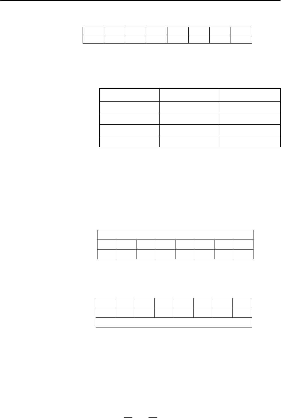
- Page 1016. CONNECTION OF I/O UNITS TO B–63783EN/01 MACHINE INTERFACE Module internal address 7 6 5 4 3 2 1 0 Yn X X X X X X X X Yn+1 X X X X X X CHB CHA Specifying a pair of values listed below for CHA and CHB causes the corresponding channel to be selected, thus enabling the A–D conversion and selection da
- Page 1026. CONNECTION OF I/O UNITS TO MACHINE INTERFACE B–63783EN/01 D If the analog input module is mounted in the space for expansion module 3 (m is the first assigned address) Module internal address 7 6 5 4 3 2 1 0 Xm+9 (odd address) Undefined Xm+10 (even address) D07 D06 D05 D04 D03 D02 D01 D00 Xm+11 (
- Page 1036. CONNECTION OF I/O UNITS TO B–63783EN/01 MACHINE INTERFACE 6.3.15 An example in which three manual pulse generators are connected is Manual Pulse shown below. Generator Connection Extension module 1 Manual pulse generators JA3 Manual pulse generator #1 (PCR–E20LMDT) (M3 screw terminal) 1 HA1 11 3
- Page 1046. CONNECTION OF I/O UNITS TO MACHINE INTERFACE B–63783EN/01 NOTE Since some pins of this connector, unlike other 20–pin connectors, have been removed, resulting in a unique pin arrangement, be careful when identifying pin numbers. See Figure 2 in Appendix B and Table C (a) in Appendix C. Recommende
- Page 1056. CONNECTION OF I/O UNITS TO B–63783EN/01 MACHINE INTERFACE However, the maximum pulse transmission distance for the manual pulse generator is 50 m. Taking this into consideration, the cable length may be extended to: 38.37 m (when two generators are used), or 25.58 m (when three generators are use
- Page 1066. CONNECTION OF I/O UNITS TO MACHINE INTERFACE B–63783EN/01 NOTE 1 Modules need to be spaced at least 32 mm apart, in which case a flat cable of about 20 mm in length is required. To install modules further away from each other, the cable length will be 20 mm plus the extra distance. Note that the
- Page 1076. CONNECTION OF I/O UNITS TO B–63783EN/01 MACHINE INTERFACE 6.3.18 When connecting a connector panel printed circuit board directly Module Installation (external module view and mounting diagram) Dimensions of connector panel printed circuit board ("0.2 mm) Board thickness 1.6 mm Square hole No. 1
- Page 1086. CONNECTION OF I/O UNITS TO MACHINE INTERFACE B–63783EN/01 When connecting a connector panel printed circuit board directly (mounting and dismounting a module) Hook (C) (A) Stopper Connector panel (B) printed circuit board Mounting the module 1. Insert the hook of the module into the square hole l
- Page 1096. CONNECTION OF I/O UNITS TO B–63783EN/01 MACHINE INTERFACE When mounting a DIN rail (external module view and mounting diagram) Mount the DIN rail here I/O interface I/O Link interface MPG interface (for extension module) NOTE Recommended connector: A02B–0098–K891 (including the following connecto
- Page 1106. CONNECTION OF I/O UNITS TO MACHINE INTERFACE B–63783EN/01 When mounting a DIN rail (mounting and dismounting a module) Hook DIN rail Stopper Slotted screwdriver Mounting the module 1. Hook the module at the upper end of the DIN rail. 2. Push the stopper into the slit located at the lower end of t
- Page 1116. CONNECTION OF I/O UNITS TO B–63783EN/01 MACHINE INTERFACE When mounting a module using screws (external module view and mounting diagram) Screw holes I/O interface I/O Link interface MPG interface (for extension module) NOTE Recommended connector: A02B–0098–K891 (including the following connector
- Page 1126. CONNECTION OF I/O UNITS TO MACHINE INTERFACE B–63783EN/01 6.3.19 DO signal reaction to a system alarm Other Notes If a system alarm occurs in a CNC using the connector panel I/O module, or if I/O Link communication between the CNC and connector panel I/O module fails, all the DO signals of the I/
- Page 1136. CONNECTION OF I/O UNITS TO B–63783EN/01 MACHINE INTERFACE Fixed addresses directly supervised by the CNC (for FS15i/150i) ADDRESS 7 6 5 4 3 2 1 0 X0006 *ESP X0008 AE2 AE1 X0011 SKIP1 When DI addresses are allocated in units of 16 bytes, starting at X0005 DI space map X0005 *ESP fixed signals X000
- Page 1146. CONNECTION OF I/O UNITS TO MACHINE INTERFACE B–63783EN/01 Alarm detection DO address Location address and bit Xm+15.0 Yn+0 Basic module Xm+15.1 Yn+1 Basic module Xm+15.2 Yn+2 Extension module 1 Xm+15.3 Yn+3 Extension module 1 Xm+15.4 Yn+4 Extension module 2 Xm+15.5 Yn+5 Extension module 2 Xm+15.6
- Page 1156. CONNECTION OF I/O UNITS TO B–63783EN/01 MACHINE INTERFACE 6.3.20 By changing the setting (rotary switch) for the expansion modules, Distribution I/O Setting connections can be made by omitting some expansion modules as shown below. Expansion module 1 Expansion module 2 Expansion module 3 Expansio
- Page 1166. CONNECTION OF I/O UNITS TO MACHINE INTERFACE B–63783EN/01 The function of the rotary switch is as follows: Setting Actual Meaning of setting position indication 0 0 This is the standard setting. The rotary switch is factory–set to this position. This setting is used when no expansion module is om
- Page 1176. CONNECTION OF I/O UNITS TO B–63783EN/01 MACHINE INTERFACE Examples of setting (When expansion module 1 is omitted) On expansion module 2, set the rotary Expansion module 1 Expansion module 2 Expansion module 3 switch to setting position 1. On expan- sion module 3, keep the rotary switch Basic mod
- Page 1186. CONNECTION OF I/O UNITS TO MACHINE INTERFACE B–63783EN/01 6.4 CONNECTION OF OPERATOR’S PANEL I/O MODULE (FOR MATRIX INPUT) 6.4.1 Overall Connection Diagram CNC I/O UNIT JD1B I/O Link JD1A JD1B JD1A CE53 MPG JA3 Machine operator’s panel MPG MPG CE54 +24 V power supply CPD1(IN) +24 V power supply C
- Page 1196. CONNECTION OF I/O UNITS TO B–63783EN/01 MACHINE INTERFACE 6.4.2 Provide the CPD1 (IN) connector, shown below, with the power Power Connection necessary for printed circuit board operation and that for DI operation. To facilitate power division, the power is output to CPD1 (OUT) exactly as it is i
- Page 1206. CONNECTION OF I/O UNITS TO MACHINE INTERFACE B–63783EN/01 6.4.3 DI/DO Connector Pin CE53 CE54 Arrangement A B A B 01 0V 0V 01 0V 0V 02 N.C. +24V 02 COM1 +24V 03 Xm+0.0 Xm+0.1 03 Xm+1.0 Xm+1.1 04 Xm+0.2 Xm+0.3 04 Xm+1.2 Xm+1.3 05 Xm+0.4 Xm+0.5 05 Xm+1.4 Xm+1.5 06 Xm+0.6 Xm+0.7 06 Xm+1.6 Xm+1.7 07
- Page 1216. CONNECTION OF I/O UNITS TO B–63783EN/01 MACHINE INTERFACE 6.4.4 DI (General–purpose Input Signal) Pin number Connection Address number CE53(B02) +24V Bit number CE54(B02) Xm+0.0 CE53(A03) RV Xm+0.1 CE53(B03) RV Xm+0.2 CE53(A04) RV Xm+0.3 CE53(B04) RV Xm+0.4 CE53(A05) RV Xm+0.5 CE53(B05) RV Xm+0.6
- Page 1226. CONNECTION OF I/O UNITS TO MACHINE INTERFACE B–63783EN/01 NOTE Xm+1.0 through Xm+1.7 are DI pins for which a common voltage can be selected. That is, by connecting the COM1 CE54(A02) pin to the +24 V power supply, a DI signal can be input with its logical state reversed. If, however, a cable is c
- Page 1236. CONNECTION OF I/O UNITS TO B–63783EN/01 MACHINE INTERFACE 6.4.5 d A maximum of 56 points are provided. DI (Matrix Input Signal) Connection *KCM1 CE53(A23) Xn+4.0 Xn+4.1 Xn+4.2 Xn+4.3 Xn+4.4 Xn+4.5 Xn+4.6 Xn+4.7 CE53(B23) Xn+5.0 Xn+5.1 Xn+5.2 Xn+5.3 Xn+5.4 Xn+5.5 Xn+5.6 Xn+5.7 *KCM2 CE53(A24) Xn+6
- Page 1246. CONNECTION OF I/O UNITS TO MACHINE INTERFACE B–63783EN/01 6.4.6 d A maximum of 56 points are provided. DO (Output Signal) Connection Pin number CE53(A25,B25) DOCOM CE54(A25,B24,B25) Address number Bit number +24V 0V +24 V stabilized power supply Yn+0.0 CE53(A07) Relay DV Yn+0.1 CE53(B07) DV Yn+0.
- Page 1256. CONNECTION OF I/O UNITS TO B–63783EN/01 MACHINE INTERFACE Pin number CE53(A25,B25) DOCOM CE54(A25,B24,B25) Address number Bit number +24V 0V +24 V stabilized power supply Yn+2.0 CE53(A15) Relay DV Yn+2.1 CE53(B15) DV Yn+2.2 CE53(A16) DV Yn+2.3 CE53(B16) DV Yn+2.4 CE53(A17) DV Yn+2.5 CE53(B17) DV
- Page 1266. CONNECTION OF I/O UNITS TO MACHINE INTERFACE B–63783EN/01 Pin number CE53(A25,B25) DOCOM CE54(A25,B24,B25) Address number Bit number +24V 0V +24 V stabilized power supply Yn+4.0 CE54(A11) Relay DV Yn+4.1 CE54(B11) DV Yn+4.2 CE54(A12) DV Yn+4.3 CE54(B12) DV Yn+4.4 CE54(A13) DV Yn+4.5 CE54(B13) DV
- Page 1276. CONNECTION OF I/O UNITS TO B–63783EN/01 MACHINE INTERFACE Pin number CE53(A25,B25) DOCOM CE54(A25,B24,B25) Address number Bit number +24V 0V +24 V stabilized power supply Yn+6.0 CE54(A19) Relay DV Yn+6.1 CE54(B19) DV Yn+6.2 CE54(A20) DV Yn+6.3 CE54(B20) DV Yn+6.4 CE54(A21) DV Yn+6.5 CE54(B21) DV
- Page 1286. CONNECTION OF I/O UNITS TO MACHINE INTERFACE B–63783EN/01 6.4.8 External View Note) Lead wires and other components are mounted on the rear Note face of the printed circuit board. Ensure that printed circuit boards are spaced 5 mm or more from one another to prevent interference. 24 V power suppl
- Page 1296. CONNECTION OF I/O UNITS TO B–63783EN/01 MACHINE INTERFACE 6.4.9 Installation specifications Specifications Ambient temperature During operation 0°C to 58°C During storage and transportation –20°C to 60°C Temperature change Max. 0.3°C/min. Relative humidity Normal : 75% or less Short term (1 month
- Page 1306. CONNECTION OF I/O UNITS TO MACHINE INTERFACE B–63783EN/01 DI (input signal) specifications (General–purpose input signal) Contact rating 30 VDC, 16 mA or more Open circuit intercontact 1 mA or less (at 26.4 V) leakage current Closed circuit intercontact 2 V or less voltage drop (including cable v
- Page 1316. CONNECTION OF I/O UNITS TO B–63783EN/01 MACHINE INTERFACE 6.4.10 Other Notes DO signal reaction to a If a system alarm occurs in the CNC using the operator’s panel I/O system alarm module, or if I/O Link communication between the CNC and operator’s panel I/O module fails, all the DO signals of th
- Page 1326. CONNECTION OF I/O UNITS TO MACHINE INTERFACE B–63783EN/01 Fixed addresses directly supervised by the CNC (for FS15i/150i) 7 6 5 4 3 2 1 0 X0006 *ESP X0008 AE2 AE1 X0011 SKIP1 When DI addresses are allocated in units of 16 bytes, starting at X0006 X0006 General–purpose *ESP fixed signal input sign
- Page 1336. CONNECTION OF I/O UNITS TO B–63783EN/01 MACHINE INTERFACE NOTE When the DO signal is in the ON state in the sequence, the ON or OFF state of the DOCOM pin determines the state of the signal, as indicated by the dotted lines in the above figure. Do not turn off the +24 V supply, provided by the CP
- Page 1346. CONNECTION OF I/O UNITS TO MACHINE INTERFACE B–63783EN/01 DO (output signal) alarm The DO driver of the I/O module is capable of detecting an overcurrent detection and measuring its own temperature. If an accident, such as connecting the cable to ground, causes an abnormal increase in the load cu
- Page 1356. CONNECTION OF I/O UNITS TO B–63783EN/01 MACHINE INTERFACE 6.5 CONNECTION OF OPERATOR’S PANEL I/O MODULE (NOT FOR MATRIX INPUT) 6.5.1 Overall Connection Diagram CNC I/O UNIT JD1B I/O LINK JD1A JD1B JD1A CE56 MPG JA3 Machine operator’s panel MPG MPG CE57 +24 V power supply CPD1(IN) +24 V power supp
- Page 1366. CONNECTION OF I/O UNITS TO MACHINE INTERFACE B–63783EN/01 6.5.2 Provide the CPD1 (IN) connector, shown below, with the power Power Connection necessary for printed circuit board operation and that for DI operation. To facilitate power division, the power is output to CPD1 (OUT) exactly as it is i
- Page 1376. CONNECTION OF I/O UNITS TO B–63783EN/01 MACHINE INTERFACE 6.5.3 DI/DO Connector Pin CE56 CE57 Arrangement A B A B 01 0V +24V 01 0V +24V 02 Xm+0.0 Xm+0.1 02 Xm+3.0 Xm+3.1 03 Xm+0.2 Xm+0.3 03 Xm+3.2 Xm+3.3 04 Xm+0.4 Xm+0.5 04 Xm+3.4 Xm+3.5 05 Xm+0.6 Xm+0.7 05 Xm+3.6 Xm+3.7 06 Xm+1.0 Xm+1.1 06 Xm+4.
- Page 1386. CONNECTION OF I/O UNITS TO MACHINE INTERFACE B–63783EN/01 6.5.4 DI (General–Purpose Input Signal) Connection Pin number Address number CE56(B01) +24V Bit number CE57(B01) Xm+0.0 CE56(A02) RV Xm+0.1 CE56(B02) RV Xm+0.2 CE56(A03) RV Xm+0.3 CE56(B03) RV Xm+0.4 CE56(A04) RV Xm+0.5 CE56(B04) RV Xm+0.6
- Page 1396. CONNECTION OF I/O UNITS TO B–63783EN/01 MACHINE INTERFACE Pin number Address number CE56(B01) +24V Bit number CE57(B01) Xm+2.0 CE56(A10) RV Xm+2.1 CE56(B10) RV Xm+2.2 CE56(A11) RV Xm+2.3 CE56(B11) RV Xm+2.4 CE56(A12) RV Xm+2.5 CE56(B12) RV Xm+2.6 CE56(A13) RV Xm+2.7 CE56(B13) RV Xm+3.0 CE57(A02)
- Page 1406. CONNECTION OF I/O UNITS TO MACHINE INTERFACE B–63783EN/01 Pin number Address number CE56(B01) +24V Bit number CE57(B01) Xm+4.0 CE57(A06) RV Xm+4.1 CE57(B06) RV Xm+4.2 CE57(A07) RV Xm+4.3 CE57(B07) RV Xm+4.4 CE57(A08) RV Xm+4.5 CE57(B08) RV Xm+4.6 CE57(A09) RV Xm+4.7 CE57(B09) RV Xm+5.0 CE57(A10)
- Page 1416. CONNECTION OF I/O UNITS TO B–63783EN/01 MACHINE INTERFACE NOTE 1 Xm+0.0 through Xm+0.7 and Xm+5.0 to Xm+5.7 are DI pins for which a common voltage can be selected. That is, by connecting the DICOM0 CE56(A14) or DICOM5 CE57 (B14) pin to the +24 V power supply, a DI signal can be input with its log
- Page 1426. CONNECTION OF I/O UNITS TO MACHINE INTERFACE B–63783EN/01 6.5.5 DO (Output Signal) Connection Pin number CE56(A24,B24,A25,B25) DOCOM CE57(A24,B24,A25,B25) Address number Bit number +24V 0V +24 V stabilized power supply Yn+0.0 CE56(A16) Relay DV Yn+0.1 CE56(B16) DV Yn+0.2 CE56(A17) DV Yn+0.3 CE56(
- Page 1436. CONNECTION OF I/O UNITS TO B–63783EN/01 MACHINE INTERFACE Pin number CE56(A24,B24,A25,B25) DOCOM CE57(A24,B24,A25,B25) Address number Bit number +24V 0V +24 V stabilized power supply Yn+2.0 CE57(A16) Relay DV Yn+2.1 CE57(B16) DV Yn+2.2 CE57(A17) DV Yn+2.3 CE57(B17) DV Yn+2.4 CE57(A18) DV Yn+2.5 C
- Page 1446. CONNECTION OF I/O UNITS TO MACHINE INTERFACE B–63783EN/01 6.5.6 For details of the connection of the manual pulse generator, see 6.3.15. Manual Pulse Generator Connection 6.5.7 External View Note) Lead wires and other components are mounted on the rear Note face of the printed circuit board. Ensu
- Page 1456. CONNECTION OF I/O UNITS TO B–63783EN/01 MACHINE INTERFACE 6.5.8 Specifications Installation specifications Ambient temperature During operation 0° to 58°C During storage and transportation –20°C to 60°C Temperature change Max. 0.3°C/min. Relative humidity Normal : 75% or less Short term (1 month
- Page 1466. CONNECTION OF I/O UNITS TO MACHINE INTERFACE B–63783EN/01 Power supply rating Module Supply voltage Current Remarks rating Operator’s 24 VDC ±10% supplied 0.3 A The total power panel I/O from the power supply +7.3 mAXDI consumption of DI module connector CPD1. The al- points is included. lowance
- Page 1476. CONNECTION OF I/O UNITS TO B–63783EN/01 MACHINE INTERFACE 6.5.9 DO signal reaction to a system alarm Other Notes If a system alarm occurs in the CNC using the operator’s panel 48/32 I/O module, or if I/O Link communication between the CNC and operator’s panel I/O module fails, all the DO signals
- Page 1486. CONNECTION OF I/O UNITS TO MACHINE INTERFACE B–63783EN/01 Fixed addresses directly supervised by the CNC (for 15i/150i) ADDRESS 7 6 5 4 3 2 1 0 X0006 *ESP X0007 AE2 AE1 X0008 SKIP1 When DI addresses are allocated in units of 16 bytes, starting at X0005 X0005 X0006 *ESP fixed signal X0007 Input si
- Page 1496. CONNECTION OF I/O UNITS TO B–63783EN/01 MACHINE INTERFACE Parallel DO (output signal) connection The DO load current can be doubled by connecting two DO points in parallel and turning them on and off simultaneously in sequence, as shown in the figure below. The maximum load current per DO point i
- Page 1506. CONNECTION OF I/O UNITS TO MACHINE INTERFACE B–63783EN/01 DO (output signal) alarm detection The DO driver of the I/O module is capable of detecting an overcurrent and measuring its own temperature. If an accident, such as connecting the cable to ground, causes an abnormal increase in the load cu
- Page 1516. CONNECTION OF I/O UNITS TO B–63783EN/01 MACHINE INTERFACE 6.6 The FANUC I/O Unit–MODEL A (“I/O Unit”) is a modular–type I/O unit. It interfaces with the machine when connected to the control unit CONNECTION OF (Series 15i/150i) via the I/O Link. One I/O unit can be configured by THE FANUC I/O mou
- Page 1526. CONNECTION OF I/O UNITS TO MACHINE INTERFACE B–63783EN/01 6.6.3 Interface modules and various types of I/O modules can be mounted to Mounting and and dismounted from the base unit easily as shown below. Dismounting Modules Mounting 1 Hang the hook at the top of the module on the groove in the upp
- Page 1536. CONNECTION OF I/O UNITS TO B–63783EN/01 MACHINE INTERFACE 6.6.4 Connection Diagram Series 15i/150i Control unit JD1A Terminator TX K1X I/O Unit–A I/O Unit–A AIF01A AIF01B JD1B JD1A JD3 JD2 JD2 CP32 PC32 24VDC 24VDC K2X K1X AIF01A AIF01B JD1B JD1A JD3 JD2 JD2 Max. CP32 PC32 16 group L 24VDC 24VDC
- Page 1546. CONNECTION OF I/O UNITS TO MACHINE INTERFACE B–63783EN/01 6.6.5 Connect the following power source to the connector CP32 of the Connecting Input interface module (AIF01A or AIF01B). Power Source D Voltage : 24VDC±10% D Current : Determine from Table 6.6.5. FCI JAPAN, LTD. tripolar connector (Brow
- Page 1556. CONNECTION OF I/O UNITS TO B–63783EN/01 MACHINE INTERFACE n : Number of the input and output points (for each module) which turn ON simultaneously D The current sum requirement for modules used in Column A should not exceed 500 mA. D The current sum requirement for modules used in Column B should
- Page 1566. CONNECTION OF I/O UNITS TO MACHINE INTERFACE B–63783EN/01 6.6.7 Details of the cables K1X, K2X and the terminator shown in the general Connecting Signal connection diagram are as follows. Cables Cable K1X Connector HONDA TSUSHIN CNC or AIF01A KOGYO CO., LTD. AIF01A PCR–E20FS JD1A JD1B (PCR–E20LMD
- Page 1576. CONNECTION OF I/O UNITS TO B–63783EN/01 MACHINE INTERFACE Cable K2X Connector HONDA TSUSHIN AIF01A KOGYO CO., LTD. AIF01B PCR–E20FS JD2 (PCR–E20LMDET) JD3 (PCR–E20LMDET) 1 S1 11 S5 1 S1 11 S5 2 *S1 12 *S5 2 *S1 12 *S5 3 S2 13 S6 3 S2 13 S6 4 *S2 14 *S6 4 *S2 14 *S6 5 S3 15 0V 5 S3 15 0V 6 *S3 16
- Page 1586. CONNECTION OF I/O UNITS TO MACHINE INTERFACE B–63783EN/01 Terminator TX AIF01B Connector JD2 (PCR–E20LMDET) HONDA TSUSHIN KOGYO CO., LTD. PCR–E20FS 1 11 2 12 TRM2 3 13 4 TRM1 14 TRM3 5 15 (a) Terminate the connector 6 16 7 17 JD2 of the last AIF01B in 8 18 a single group with the terminator. 9 19
- Page 1596. CONNECTION OF I/O UNITS TO B–63783EN/01 MACHINE INTERFACE 6.6.8 For an external connecting method, there are two types of I/O modules : Connecting with I/O one with a terminal block, and one with a connector. The terminal block is a removable type. Modules Terminal block type Connector type Input
- Page 1606. CONNECTION OF I/O UNITS TO MACHINE INTERFACE B–63783EN/01 Cautionary points when D Wiring material :AWG22 – 18 (0.3 – 0.75mm2) wiring terminal block A wire as thin as possible is recommended. type D Crimp style terminal : M3.5 Crimp style terminal with no insulation sleeve and a short distance “A
- Page 1616. CONNECTION OF I/O UNITS TO B–63783EN/01 MACHINE INTERFACE Digital output modules ModĆ Points External Output Rated Rated PolarĆ LED ule Points /comĆ connecĆ Fuse type voltage current ity display name mon tion AOD 12–24 Terminal pro- 2A NEG 8 8 provided 08C VDC block vided AOD Terminal pro- 2A POS
- Page 1626. CONNECTION OF I/O UNITS TO MACHINE INTERFACE B–63783EN/01 6.6.10 Correspondence Bit between I/O Signals Address in the module and Addresses in a #7 #6 #5 #4 #3 #2 #1 #0 Module Module of 8 0 A7 A6 A5 A4 A3 A2 A1 A0 points Module of 16 points 1 B7 B6 B5 B4 B3 B2 B1 B0 2 C7 C6 C5 C4 C3 C2 C1 C0 Modu
- Page 1636. CONNECTION OF I/O UNITS TO B–63783EN/01 MACHINE INTERFACE 6.6.11 Determine the number of I/O points for the I/O Unit –MODEL A using Number of Points for the following. I/O Unit–MODEL A D Output points Sum of the actual output Occupied output points points in a group 0 to 32 → 32 points 40 to 64 →
- Page 1646. CONNECTION OF I/O UNITS TO MACHINE INTERFACE B–63783EN/01 6.7 The machine operator’s panel interface unit (A16B–2201–0110) is connected to the control unit through the I/O Link and is used for CONNECTION OF interfacing with the machine operator’s panel. MACHINE It features interfaces with matrix
- Page 1656. CONNECTION OF I/O UNITS TO B–63783EN/01 MACHINE INTERFACE Analog signal inputs D Two inputs (input voltage: 0 to +10 V) D Input voltages are converted from analog to digital. The resulting five bits of data are sent to the CNC through the FANUC I/O Link. D The analog signal input function can be
- Page 1666. CONNECTION OF I/O UNITS TO MACHINE INTERFACE B–63783EN/01 6.7.2 System Configuration CNC Machine operator’s panel Machine operator’s interface unit panel Note 2 FANUC JD1B CM26 Matrix DI/DO I/O Link (I/O Link) *ESP, OTR, and general–purpose JD1A CM15 DI/DO Other machine interface CM16 General–pur
- Page 1676. CONNECTION OF I/O UNITS TO B–63783EN/01 MACHINE INTERFACE 6.7.3 Signal Assignment Connector pin signal assignment CM15 (General DI/DO) CM16 (General DI/DO) CM17 (General DI/DO) A B A B A B 01 +5E DI06 01 DI20 DI22 01 0V 0V 02 0V DO06 02 DI24 +5E 02 DO20 DO21 03 +5E DI07 03 DI23 DI21 03 DO22 DO23
- Page 1686. CONNECTION OF I/O UNITS TO MACHINE INTERFACE B–63783EN/01 JD1A (FANUC I/O Link : NEXT SLAVE) 10 20 +5V 9 +5V 19 8 18 +5V 7 17 6 16 0V 5 15 0V 4 *TXB 14 0V 3 TXB 13 0V 2 *RXB 12 0V 1 RXB 11 0V JD1B (FANUC I/O Link : BEFORE SLAVE) 10 20 +5V 9 +5V 19 8 18 +5V 7 17 6 16 0V 5 15 0V 4 *TXA 14 0V 3 TXA
- Page 1696. CONNECTION OF I/O UNITS TO B–63783EN/01 MACHINE INTERFACE 6.7.4 Interface General–purpose DI +5E DI00 to DI37 RV 0V Input signal specifications Contact rating 5VDC, 3.2mA or higher Leakage current between open contacts 0.2mA or lower (5 VDC) Voltage drop across closed contacts 0.75V or lower Gene
- Page 1706. CONNECTION OF I/O UNITS TO MACHINE INTERFACE B–63783EN/01 Matrix DI D Key switch addresses See Subsec. 6.7.5 for the corresponding PMC addresses. CM26–A06 KY07 KY06 KY05 KY04 KY03 KY02 KY01 KY00 BZ0 *KYC0 CM26–B06 KY17 KY16 KY15 KY14 KY13 KY12 KY11 KY10 BZ1 *KYC1 CM26–A07 KY27 KY26 KY25 KY24 KY23
- Page 1716. CONNECTION OF I/O UNITS TO B–63783EN/01 MACHINE INTERFACE D Mode selection - Preventing malfunctions that may be caused by detouring current When there are three or more matrix DI points, detouring current can cause a nonexistent DI input to be falsely detected as existing. As shown below, if KY0
- Page 1726. CONNECTION OF I/O UNITS TO MACHINE INTERFACE B–63783EN/01 - This PCB can raise a confirmation sound when a key is pressed. The condition to raise an audible alarm is set in 8–bit units, or in *KYCn units. If *BZMD and common *KYCn are disconnected, a KYnx input causes a sound to generate. If they
- Page 1736. CONNECTION OF I/O UNITS TO B–63783EN/01 MACHINE INTERFACE D Signal specification Contact rating 6VDC, 2mA or higher Leakage current between open contacts 0.2mA or lower (6VDC) Voltage drop across closed contacts 0.9V or lower (1 mA) Note ) NOTE This voltage must be maintained even when detour pre
- Page 1746. CONNECTION OF I/O UNITS TO MACHINE INTERFACE B–63783EN/01 Matrix DO D LED addresses See Subsec. 6.7.5 for the corresponding PMC addresses. LC4L CM26–A24 LC3L CM26–A23 LC2L CM26–A22 LC1L CM26–A21 CM26–A13 L1L0 *LD0 CM26–A14 L1L1 *LD1 *LD2 CM26–A15 L1L2 *LD3 CM26–A16 L1L3 *LD4 CM26–A17 L1L4 *LD5 CM
- Page 1756. CONNECTION OF I/O UNITS TO B–63783EN/01 MACHINE INTERFACE CM26–B24 LC4H CM26–B23 LC3H CM26–B22 LC2H CM26–B21 LC1H CM26–B13 L1H0 *LD8 CM26–B14 L1H1 *LD9 CM26–B15 L1H2 *LD10 CM26–B16 L1H3 *LD11 CM26–B17 L1H4 *LD12 CM26–B18 L1H5 *LD13 CM26–B19 L1H6 *LD14 CM26–B20 L1H7 *LD15 L2H0 L2H1 L2H2 L2H3 L2H4
- Page 1766. CONNECTION OF I/O UNITS TO MACHINE INTERFACE B–63783EN/01 D Signal specifications The LEDs must have the following rating Forward voltage 2.4V max (If=5mA)(Typical value) Forward current 30mA max Reverse voltage 3V max Interface for manual pulse generator D Connection of connector One interface i
- Page 1776. CONNECTION OF I/O UNITS TO B–63783EN/01 MACHINE INTERFACE Analog signal inputs Analog inputs received from the outside are forwarded without change to output terminals. D Connection diagram Analog inputs from the spindle amp being output for load meter and speed (example) meter indications. LM Sp
- Page 1786. CONNECTION OF I/O UNITS TO MACHINE INTERFACE B–63783EN/01 D Emergency stop A signal generated by the emergency stop switch on the machine operator’s panel can be sent to the power magnetics cabinet. (This signal cannot be sent to the CNC through the FANUC I/O Link.) Emergency stop signal A09 17 *
- Page 1796. CONNECTION OF I/O UNITS TO B–63783EN/01 MACHINE INTERFACE 6.7.5 PMC Addresses Scope in which PMC addresses can be used BIT NUMBER I/O Link allocation PMC 7 6 5 4 3 2 1 0 128/128 256/256 ADDRESS DI+00 FUSE DI+01 KY07 KY06 KY05 KY04 KY03 KY02 KY01 KY00 DI+02 KY17 KY16 KY15 KY14 KY13 KY12 KY11 KY10
- Page 1806. CONNECTION OF I/O UNITS TO MACHINE INTERFACE B–63783EN/01 6.7.6 D Use flat cables for connectors CM15, CM16, CM17, and CM26. Major Connection When splitting and connecting flat cables to the machine operator’s panel or other equipment, be careful not to break or short the Precautions conductors.
- Page 1816. CONNECTION OF I/O UNITS TO B–63783EN/01 MACHINE INTERFACE 6.7.8 Connector Connector Major use Specification (on the Cable Side) CM15, General–purpose HIF3BA–34D–2.54R : Specifications CM16, DI/DO Manufactured by HIROSE ELECTRIC CM17 CO., LTD. CNA1 Relay terminal PCR–E20FS : (to the machine) Manuf
- Page 1826. CONNECTION OF I/O UNITS TO MACHINE INTERFACE B–63783EN/01 6.7.9 Machine Operator’s Panel Interface Unit Dimension Diagram (Including Connector Locations) 89 22 CM26 A1 B25 15 CPD1 11 A1 17 10 60 CNB1 150 CM17 CNA1 9 B17 41 75 16 JD1B 1 CA40 CM16 CM15 A1 JD1A A1 22 20 B17 B17 40 124 89 26 310 Unit
- Page 1836. CONNECTION OF I/O UNITS TO B–63783EN/01 MACHINE INTERFACE 6.7.10 Machine Operator’s Panel Interface Unit Mounting Dimension Diagram Mounting hole position 20 CM26 18 150 CM17 110 114 Hole for connecting to a ground 4.5f CM16 CM15 20 18 296 310 Fasten the PCB with four M4 screws. Unit : mm 171
- Page 1846. CONNECTION OF I/O UNITS TO MACHINE INTERFACE B–63783EN/01 Sheet fixing area It is possible to fix the sheet, spacer, etc. only in the area shown in the (mounting face side) diagram below. 15 12 10 CM26 10 10 8 25 18 7 CM17 130 7 5 130 3 CM16 CM15 20 14 10 8 10 10 12 14 NOTE Applied to the PCB ver
- Page 1856. CONNECTION OF I/O UNITS TO B–63783EN/01 MACHINE INTERFACE 6.7.11 Fuse Mounting Position CM26 FU1 CPD1 FU3 FU2 CM17 JD1A JD1B CM16 CM15 FU1 : +24V fuse (general–purpose DO, this supplies printed board power protection) FU2 : +5V fuse (IC power, manual pulse generator protection) FU3 : +5E fuse (ge
- Page 1866. CONNECTION OF I/O UNITS TO MACHINE INTERFACE B–63783EN/01 6.8 A connection unit (A20B–1005–0310 or A20B–1003–0200) is connected to the control unit of the Series 15i/150i via FANUC I/O Link CONNECTING THE and used for interfacing with the machine. CONNECTION UNIT Electrical interfaces and pin ass
- Page 1876. CONNECTION OF I/O UNITS TO B–63783EN/01 MACHINE INTERFACE Connection unit 1 A20B–1005–0310 Series 15i/150i control unit or To the next device I/O unit If there is no equipment beyond this connection unit, JD1A can remain open. 3–pin connector (brown) manufactured by FCI Japan Housing: SMS3PNS–5 C
- Page 1886. CONNECTION OF I/O UNITS TO MACHINE INTERFACE B–63783EN/01 6.8.1 (a) Between CP52 and CP55 Connecting Connection Unit 1 and Connection Unit 2 CP52 CP55 1 2 3 4 5 6 1 2 3 4 5 6 +5 V +5 V 0V 0V +24 V +24 N +5 V +5 V 0V 0V +24 V +24 N Connectors SMS6PN–5 Use a 30/0.18 (0.75 mm2) wire or thicker for t
- Page 1896. CONNECTION OF I/O UNITS TO B–63783EN/01 MACHINE INTERFACE (b) Between CDD1 and CDD2 Connection Unit 1 Connection Unit 2 CDD1 CDD2 FAP–50–1 FAP–50–1 A01 0V B01 0V A01 0V B01 0V A02 B02 A02 B02 A03 B03 A03 B03 A04 0V B04 A04 0V B04 A05 B05 A05 B05 Cable A06 B06 0V A06 B06 0V A07 *D7 B07 *D6 A07 *D7
- Page 1906. CONNECTION OF I/O UNITS TO MACHINE INTERFACE B–63783EN/01 6.8.2 Input signals for the connection unit conform to a non–insulation type Input Signal interface. There are two input types: Direct current input signal A and direct current input signal B. Regulations for the (1) Direct current input s
- Page 1916. CONNECTION OF I/O UNITS TO B–63783EN/01 MACHINE INTERFACE (2) Direct current input signal B Direct current input signal B is a signal sent from the machine to the CNC and used at high speed. (a) The contacts on the machine must meet the following requirements: Contact capacity: 30 VDC, 16 mA or m
- Page 1926. CONNECTION OF I/O UNITS TO MACHINE INTERFACE B–63783EN/01 6.8.3 (1) Connection unit 1 Connector Pin Assignment for the Connection Unit C01 MR–50RMA 1 2 3 4 5 6 7 8 9 10 11 12 13 14 15 16 17 18 DIB5 DIB1 DIB6 DI44 DI40 DI45 DI16 DI60 19 20 21 22 23 24 25 26 27 28 29 30 31 32 0V DIB7 DIB4 DI26 DI37
- Page 1936. CONNECTION OF I/O UNITS TO B–63783EN/01 MACHINE INTERFACE (2) Connection unit 2 C09 MR–50RMA 1 2 3 4 5 6 7 8 9 10 11 12 13 14 15 16 17 18 DI75 DI71 DI76 DI104 DI100 DI105 DID6 DI102 19 20 21 22 23 24 25 26 27 28 29 30 31 32 0V DI177 DI174 DIE6 DIF7 DIC6 DIF3 DI110 DI122 DI111 33 34 35 36 37 38 39
- Page 1946. CONNECTION OF I/O UNITS TO MACHINE INTERFACE B–63783EN/01 6.8.4 Details of the Connection between the Connection Unit and the Machine Connection unit 1 Address number Connector pin Bit number number Direct current input signal A NOTE The machine tool builder can determine address number n. 182
- Page 1956. CONNECTION OF I/O UNITS TO B–63783EN/01 MACHINE INTERFACE Connection unit 1 Address number Connector pin Bit number number Direct current input signal A NOTE The machine tool builder can determine address number n. 183
- Page 1966. CONNECTION OF I/O UNITS TO MACHINE INTERFACE B–63783EN/01 Connection unit 1 Address number Connector pin Bit number number Direct current input signal A NOTE The machine tool builder can determine address number n. DI82 to DI80 are assigned to two connector pins each. 184
- Page 1976. CONNECTION OF I/O UNITS TO B–63783EN/01 MACHINE INTERFACE Connection unit 1 Address number Connector pin Bit number number Direct current input signal B NOTE The machine tool builder can determine address number n. The common voltage for DIB7 to DIB0 can be selected from +24 V and 0 V by the wiri
- Page 1986. CONNECTION OF I/O UNITS TO MACHINE INTERFACE B–63783EN/01 Connection unit 1 Connector pin Bit number number Address number Direct current input signal A NOTE The machine tool builder can determine address number m. The common voltages for DO05 to DO00 are connected in connection unit 1 (COM1). Th
- Page 1996. CONNECTION OF I/O UNITS TO B–63783EN/01 MACHINE INTERFACE Connection unit 1 Connector pin Bit number number Address number Direct current input signal A NOTE The machine tool builder can determine address number m. 187
- Page 2006. CONNECTION OF I/O UNITS TO MACHINE INTERFACE B–63783EN/01 Connection unit 1 Connector pin Bit number number Address number Direct current input signal A NOTE The machine tool builder can determine address number m. The common voltages for DO21, DO20, and DO37 to DO30 are connected in connection u
- Page 2016. CONNECTION OF I/O UNITS TO B–63783EN/01 MACHINE INTERFACE Connection unit 1 Bit number Connector pin Address number number Direct current input signal A NOTE The machine tool builder can determine address number m. The common voltages for DO22 and DO67 to DO60 are connected in connection unit 1 (
- Page 2026. CONNECTION OF I/O UNITS TO MACHINE INTERFACE B–63783EN/01 Connection unit 1 Bit number Connector pin num- Address number ber C05 (15) Direct current input signal A NOTE The machine tool builder can determine address number m. The common voltages for DO47 to DO40 and DO53 to DO50 are connected in
- Page 2036. CONNECTION OF I/O UNITS TO B–63783EN/01 MACHINE INTERFACE Connection unit 2 Address number Connector pin number Bit number Direct current input signal A NOTE The machine tool builder can determine address number n. 191
- Page 2046. CONNECTION OF I/O UNITS TO MACHINE INTERFACE B–63783EN/01 Connection unit 2 Address number Connector pin number Bit number Direct current input signal A NOTE The machine tool builder can determine address number n. 192
- Page 2056. CONNECTION OF I/O UNITS TO B–63783EN/01 MACHINE INTERFACE Connection unit 2 Address number Connector pin number Bit number Direct current input signal A NOTE The machine tool builder can determine address number n. DI142 to DI140 are assigned to two connector pins each. 193
- Page 2066. CONNECTION OF I/O UNITS TO MACHINE INTERFACE B–63783EN/01 Connection unit 2 Address number Connector pin number Bit number Direct current input signal A NOTE The machine tool builder can determine address number n. The common voltage for DI177 to DI170 can be selected from +24 V and 0 V by the wi
- Page 2076. CONNECTION OF I/O UNITS TO B–63783EN/01 MACHINE INTERFACE Connection unit 2 Bit number Connector pin num- ber Address number Direct current input signal A NOTE The machine tool builder can determine address number m. The common voltages for DO85 to DO80 are connected in connection unit 2 (COM19).
- Page 2086. CONNECTION OF I/O UNITS TO MACHINE INTERFACE B–63783EN/01 Connection unit 2 Bit number Connector pin num- ber Address number Direct current input signal A NOTE The machine tool builder can determine address number m. 196
- Page 2096. CONNECTION OF I/O UNITS TO B–63783EN/01 MACHINE INTERFACE Connection unit 2 Bit number Connector pin num- ber Address number Direct current input signal A NOTE The machine tool builder can determine address number m. The common voltages for DOA1, DOA0, and DOB7 to DOB0 are connected in connection
- Page 2106. CONNECTION OF I/O UNITS TO MACHINE INTERFACE B–63783EN/01 Connection unit 2 Bit number Connector pin num- ber Address number Direct current input signal A NOTE The machine tool builder can determine address number m. The common voltages for DOA2 and DOE7 to DOE0 are connected in connection unit 2
- Page 2116. CONNECTION OF I/O UNITS TO B–63783EN/01 MACHINE INTERFACE Connection unit 2 Bit number Connector pin num- Address number ber Direct current input signal A NOTE The machine tool builder can determine address number m. The common voltages for DOC7 to DOC0 and DOD3 to DOD0 are connected in connectio
- Page 2126. CONNECTION OF I/O UNITS TO MACHINE INTERFACE B–63783EN/01 6.8.5 External View of the Connection Unit 200
- Page 2136. CONNECTION OF I/O UNITS TO B–63783EN/01 MACHINE INTERFACE 6.9 The operator’s panel connection unit (A16B–2200–0660, 0661) is connected to the Series 15i/150i control unit through the FANUC I/O CONNECTION OF Link and is used for interfacing with the machine operator’s panel. OPERATOR’S PANEL The e
- Page 2146. CONNECTION OF I/O UNITS TO MACHINE INTERFACE B–63783EN/01 6.9.1 Input signals for the operator’s panel connection unit conform to a Input Signal non–insulation type interface. The input type is direct current input signal A. Regulations for the (1) Direct current input signal A Operator’s Panel D
- Page 2156. CONNECTION OF I/O UNITS TO B–63783EN/01 MACHINE INTERFACE 6.9.2 The output signals from the operator’s panel connection unit are used for Output Signal driving lamps and light emitting diodes on the machine operator’s panel. An NPN transistor is used as a driver. The output type is direct current
- Page 2166. CONNECTION OF I/O UNITS TO MACHINE INTERFACE B–63783EN/01 (b) Output circuit ÅÅÅÅ Machine CNC ÅÅÅÅ + ÅÅÅÅ Relay Regulated power supply on the machine - Transistor output circuit (c) When an inductive load such as a relay is connected to the machine, mount a spark killer as near the load as possib
- Page 2176. CONNECTION OF I/O UNITS TO B–63783EN/01 MACHINE INTERFACE 6.9.3 Connector Layout for Sink Output Operator’s Panel Connection Unit Address Note) DI80 to DIB7 can be used only for the A16B–2200–0660. NOTE Address No. n can be decided by machine tool builders. 205
- Page 2186. CONNECTION OF I/O UNITS TO MACHINE INTERFACE B–63783EN/01 Address Note) DO40 to DO77 can be used only for the A16B–2200–0660. NOTE Address No. n can be decided by machine tool builders. 206
- Page 2196. CONNECTION OF I/O UNITS TO B–63783EN/01 MACHINE INTERFACE 6.9.4 Details of the Connection between the Sink Output Operator’s Panel Connection Unit and the Machine Operator’s panel connection unit Connector terminal number Address number Bit number Direct current input signal A NOTE The machine to
- Page 2206. CONNECTION OF I/O UNITS TO MACHINE INTERFACE B–63783EN/01 Operator’s panel connection unit Connector terminal number Address number Bit number Direct current input signal A NOTE The machine tool builder can determine address number p. 208
- Page 2216. CONNECTION OF I/O UNITS TO B–63783EN/01 MACHINE INTERFACE Operator’s panel connection unit Connector terminal number Address number Bit number Direct current input signal A NOTE The machine tool builder can determine address number p. 209
- Page 2226. CONNECTION OF I/O UNITS TO MACHINE INTERFACE B–63783EN/01 Operator’s panel connection unit Connector terminal number Address number Bit number Direct current input signal A NOTE The machine tool builder can determine address number p. 210
- Page 2236. CONNECTION OF I/O UNITS TO B–63783EN/01 MACHINE INTERFACE Operator’s panel connection unit Connector terminal number Example of connection Bit number (*) Address number Direct current input signal A +24 V regulated power supply NOTE (*) The machine tool builder can determine address number q. The
- Page 2246. CONNECTION OF I/O UNITS TO MACHINE INTERFACE B–63783EN/01 Operator’s panel connection unit Connector terminal number Example of connection Bit number Address number Direct current input signal A +24 V regulated power supply NOTE The machine tool builder can determine address number q. The common
- Page 2256. CONNECTION OF I/O UNITS TO B–63783EN/01 MACHINE INTERFACE Operator’s panel connection unit Connector terminal number Example of connection Bit number Address number Direct current input signal A +24 V regulated power supply NOTE The machine tool builder can determine address number q. The common
- Page 2266. CONNECTION OF I/O UNITS TO MACHINE INTERFACE B–63783EN/01 6.9.5 External View of Sink Output Operator’s Panel Connection Unit Approx. Fig. 6.9.5 External view of operator’s panel connection unit The following LEDs and fuses are mounted on this printed circuit board. [LEDs] DB1 (GREEN PILOT): Ligh
- Page 2276. CONNECTION OF I/O UNITS TO B–63783EN/01 MACHINE INTERFACE 6.10 The source output operator’s panel connection unit (A16B–2202–0730, or –0731) is connected to Series 15i/150i control units by the FANUC I/O CONNECTION OF Link, and functions as the interface with the machine tool operator’s SOURCE OU
- Page 2286. CONNECTION OF I/O UNITS TO MACHINE INTERFACE B–63783EN/01 6.10.1 The input signal to the source output operator’s panel connection unit is Source Output input over a non–insulated interface, and is called “DC input signal A.” Operator’s Panel (1) DC input signal A DC input signal A is sent to the
- Page 2296. CONNECTION OF I/O UNITS TO B–63783EN/01 MACHINE INTERFACE (c) Circuit of common switchable input receiver Source output operator’s panel connection unit Sink–type connection: safety standard Receiver compliant (24 V common) output Input signal Filter and level signal conversion circuit Contact DI
- Page 2306. CONNECTION OF I/O UNITS TO MACHINE INTERFACE B–63783EN/01 Source–type input signals are logic “1” when the contact is open, and logic “0” when closed. CAUTION If the output signal line falls to ground when the input signal is source–type (0 V common), the state is the same when the contact is clo
- Page 2316. CONNECTION OF I/O UNITS TO B–63783EN/01 MACHINE INTERFACE (b) Output signal driver Eight signals are output from each of the output signal driver elements used on this operator’s panel connection unit. The current of each output signal is monitored in the driver element. When overcurrent is detec
- Page 2326. CONNECTION OF I/O UNITS TO MACHINE INTERFACE B–63783EN/01 If the CNC diagnoses that output does not turn ON even though it is ON, a probable cause is that overloading of that output or other output in the same element is causing the eight outputs of that element to stay OFF. If this is the case,
- Page 2336. CONNECTION OF I/O UNITS TO B–63783EN/01 MACHINE INTERFACE CAUTION If the output signal falls to ground when the output signal is sink–type (0 V common), the output signal stays ON. For this reason, sink–type output signals are not recommended for ensuring safety. By CE–marking compliancy, source–
- Page 2346. CONNECTION OF I/O UNITS TO MACHINE INTERFACE B–63783EN/01 System alarms generated by the above alarms are as follows. For details, refer to “FANUC Series 15i/150i–MODEL A Maintenance Manual (B–63325EN).” “NMI SLC aa(bb)” Example “NMI SLC 03(41)” (aa: XXXXXX11 Binary bits 0 and 1 are “1”. Other bi
- Page 2356. CONNECTION OF I/O UNITS TO B–63783EN/01 MACHINE INTERFACE 6.10.4 (a) Connector pin assignment Connector Pin Assignment Addresses of Source Output Operator’s Panel Connection Unit CM51 CM52 1 DI00 33 DICMN1 1 DI60 33 0V 2 DI03 34 DI02 2 DI63 34 DI62 19 DI01 19 DI61 3 DI06 35 DI05 3 DI66 35 DI65 20
- Page 2366. CONNECTION OF I/O UNITS TO MACHINE INTERFACE B–63783EN/01 DICMN1, DICMN2 : DI (input) common switching terminals. Normally, short with 0 V before use. +24 V : +24 VDC (output) terminal. Do not connect to inputs other than DI signal inputs on the operator’s panel connection unit. DOCOM : DO driver
- Page 2376. CONNECTION OF I/O UNITS TO B–63783EN/01 MACHINE INTERFACE For details on address assignment, refer to the “FANUC PMC–MODEL N/NA PROGRAMMING MANUAL (Ladder Language) (B–61013E)” or “FANUC PMC–MODEL NB PROGRAMMING MANUAL (Ladder Language) (B–61863E).” 6.10.5 Details of Machine Side Connections of S
- Page 2386. CONNECTION OF I/O UNITS TO MACHINE INTERFACE B–63783EN/01 Control panel connection unit Address number Connector number Connection example Bit number CM52 (21) X p+6.7 DI67 RV DC input R signal A +24 V +24 V CM51 (18), CM52 (18) NOTE The machine tool builder can determine address number p. 226
- Page 2396. CONNECTION OF I/O UNITS TO B–63783EN/01 MACHINE INTERFACE Control panel connection unit Address number Connector number Connection example Bit number CM52 (31) X p+10.7 DIA7 RV DC input R signal A +24 V +24 V CM51 (18), CM52 (18) NOTE The machine tool builder can determine address number p. 227
- Page 2406. CONNECTION OF I/O UNITS TO MACHINE INTERFACE B–63783EN/01 Connection example Control panel connection unit CMB3 (17) CMB3 (50) Stabilized pow- CMB4 (20) DOCOM er supply +24 V +24 V 0 V Address number +5 V Bit number DAL1 ALM Y q+0.7 R Lamp DC input CMB3 (21) D007 signal A DV +5 V +24 V ALM DAL2 D
- Page 2416. CONNECTION OF I/O UNITS TO B–63783EN/01 MACHINE INTERFACE Connection example Control panel connection unit CMB3 (17) Stabilized pow- CMB3 (50) er supply CMB4 (20) DOCOM +24 V +24 V 0 V Address number +5 V Bit number DAL4 ALM Lamp Y q+3.7 R DC input CMB3 (44) D037 signal A DV +5 V +24 V ALM DAL5 D
- Page 2426. CONNECTION OF I/O UNITS TO MACHINE INTERFACE B–63783EN/01 Connection example Control panel connection unit CMB3 (17) CMB3 (50) Stabilized pow- CMB4 (20) er supply +24 V DOCOM +24 V 0 V Address number +5 V Bit number DAL7 ALM Y q+6.7 R Lamp DC input CMB4 (03) D067 signal A DV +5V +24 V ALM DAL8 DV
- Page 2436. CONNECTION OF I/O UNITS TO B–63783EN/01 MACHINE INTERFACE Details of machine side connections of source output operator’s panel connection unit (DI common switchable DI) Control panel connection unit Address number Connector number Connection example Bit number CM51 (21) X p+0.7 DI07 RV DC input
- Page 2446. CONNECTION OF I/O UNITS TO MACHINE INTERFACE B–63783EN/01 6.10.6 External Dimensions of Source Output Operator’s Panel Connection Unit CP1 CRT A16B–2202–0730 (DI96/DO64) A16B–2202–0731 (DI64/DO32) Approx Fig. 6.10.6 External dimensions of source output operator’s panel connection unit The followi
- Page 2456. CONNECTION OF I/O UNITS TO B–63783EN/01 MACHINE INTERFACE 6.11 The addresses of the emergency stop signal (*ESP), skip signal (SKIP1), and measured position reached signals (AE1 and AE2), which are input ADDRESS–FIXED from the machine, are fixed. SIGNALS Signal Address Emergency stop signal *ESP
- Page 2466. CONNECTION OF I/O UNITS TO MACHINE INTERFACE B–63783EN/01 6.12 CONNECTION TO THE MACHINE OPERATOR’S PANEL 6.12.1 Machine operator’s panel is connected with i series CNC by I/O Link, Overview which is composed by some following operator’s panels. Main panel A/A1 This operator’s panel incorporated
- Page 2476. CONNECTION OF I/O UNITS TO B–63783EN/01 MACHINE INTERFACE 290 10.4”LCD 220 600 Main panel A 300 Sub panel A 80 Unit=mm Main panel B Sub panel B Main panel B Sub panel C 235
- Page 2486. CONNECTION OF I/O UNITS TO MACHINE INTERFACE B–63783EN/01 6.12.2 Total Connection Diagram MDI Unit LCD unit or CNC control unit LCD unit CNK1 Main panel A/B/A1/B1 MDI(CA55) MDI Main CPU MDI(JA2) CNK1 Keyboard CM68 General–purpose DI/DO I/O Link(JD1A) JD1B CM69 JD1A JA3 MPG Next I/O unit MPG MPG P
- Page 2496. CONNECTION OF I/O UNITS TO B–63783EN/01 MACHINE INTERFACE 6.12.3 Each Connections 6.12.3.1 Pin assignment CA64 (Power source) CA65 (Power magnetic cabinet) 3 2 0V 1 +24V A01 EON B01 EOFF 6 5 0V 4 +24V A02 COM1 B02 COM2 Recommended connector for cable: A03 *ESP B03 ESPCM1 Housing : AMP 1–178288–3
- Page 2506. CONNECTION OF I/O UNITS TO MACHINE INTERFACE B–63783EN/01 NOTE 1 Input/output Pins shaded by are in pairs. Only one in each pair is usable. 2 Pins shaded by are those for forwarding signals. Pins with the same name are connected directly to one another. JA3 (Manual pulse generator) JA58 (Pendant
- Page 2516. CONNECTION OF I/O UNITS TO B–63783EN/01 MACHINE INTERFACE 6.12.3.2 To the connector CA64 (IN) shown in the figure below, connect the Power supply required power for operating the operator’s panel and the power for general–purpose DI. For easier power supply branching, the power connection supplie
- Page 2526. CONNECTION OF I/O UNITS TO MACHINE INTERFACE B–63783EN/01 6.12.3.3 MDI connection LCD unit or Main CPU Machine operator’s panel CA55 or JA2 CNK1 (PCR E20MDK–SL–A) P A B 1 *KEY00 11 *KEY01 1 *KEY00 *KEY02 2 *KEY02 12 *KEY03 2 *KEY01 *KEY03 3 *KEY04 13 *KEY05 3 *KEY04 *KEY06 4 *KEY06 14 *KEY07 4 *K
- Page 2536. CONNECTION OF I/O UNITS TO B–63783EN/01 MACHINE INTERFACE 6.12.3.4 I/O Link connection Control unit preceding slave unit Main panel A/B/A1/B1 JD1A JD1B (PCR–E20MDK–SL–A) JD1B (PCR–E20MDK–SL–A) JD1A 1 SIN 11 0V 1 SIN 11 0V 2 *SIN 12 0V 2 *SIN 12 0V 3 SOUT 13 0V 3 SOUT 13 0V Next slave 4 *SOUT 14 0
- Page 2546. CONNECTION OF I/O UNITS TO MACHINE INTERFACE B–63783EN/01 6.12.3.5 A signal generated by the emergency stop switch on the machine Emergency stop signal operators panel can be sent to the power magnetic cabinet. (This signal cannot be sent to the FANUC I/O Link.) connection When MTB uses the Sub p
- Page 2556. CONNECTION OF I/O UNITS TO B–63783EN/01 MACHINE INTERFACE 6.12.3.7 DI (input signal) connection Pin number +24V CM68(A1),CM69(A1), JA58(10),JA58(19) Address number Bit Sub panel A CM65(A04) D Rotary switch Xm+0.0 CM65(B05) A (SA1) RV Xm+0.1 CM65(A03) F RV Xm+0.2 CM65(A05) B RV Xm+0.3 CM65(B03) E
- Page 2566. CONNECTION OF I/O UNITS TO MACHINE INTERFACE B–63783EN/01 NOTE Connection of Xm+0.0 to Xm+0.7, Xm+1.0 to Xm+1.4 shows when the Sub panel A is used. Address number Pin number +24V Bit JA58(17) Xm+2.0 CM68(A03) RV JA58(8) Xm+2.1 CM68(B03) RV JA58(3) Xm+2.2 CM68(A04) RV JA58(4) Xm+2.3 CM68(B04) RV J
- Page 2576. CONNECTION OF I/O UNITS TO B–63783EN/01 MACHINE INTERFACE NOTE 1 Xm+3.0–3.7 have a common line that is possible to select the source/sink type. If DICOM (CM69–B06pin) is connected to +24V, the DI signal logic is negative. But in this connection, if the DI signal wires happen to drop the ground le
- Page 2586. CONNECTION OF I/O UNITS TO MACHINE INTERFACE B–63783EN/01 6.12.3.8 DO (output signal) connection Pin number DOCOM CM68 ( A10 ),CM69(A10) Address No. Bit +24V 0V +24V Power JA58 (7 ) Yn + 5.3 CM 68 ( A08 ) Relay DV Yn + 5.7 DV CM 68 ( B08 ) Yn + 6.3 DV CM 68 ( A09 ) Yn + 6.7 DV CM 68 ( B09 ) Yn +
- Page 2596. CONNECTION OF I/O UNITS TO B–63783EN/01 MACHINE INTERFACE Main panel A, B, A1, B1 JA3 3 4 5 6 +5V 0V HA1 HB1 1 HA1 11 Manual pulse generator # 1 2 HB1 12 0V (M3 Screw) 3 HA2 13 3 4 5 6 4 HB2 14 0V +5V 0V HA1 HB1 5 HA3 15 Manual pulse generator # 2 6 HB3 16 0V (M3 Screw) 7 17 3 4 5 6 8 18 +5V +5V
- Page 2606. CONNECTION OF I/O UNITS TO MACHINE INTERFACE B–63783EN/01 0.1 R 2L 0.1 : MPG power supply current 0.1A 0.2w R : Resistance per wire length (Ω/m) m m : Wire Number(Both 0V and 5V) L : Cable length(m) Because m Lv R Example: In case of cable A66L–0001–0286 It has 3 pairs signal wires and 6 power li
- Page 2616. CONNECTION OF I/O UNITS TO B–63783EN/01 MACHINE INTERFACE And the receiver circuit is as follows. +5V Filter 10K W R Connector - Internal + receiver circuit C 0V 0V VIH,VIL level at Connector pin If Vin low to high, VIH must be higher than 3.7V. If Vin high to low, VIL must be lower than 1.5V. (2
- Page 2626. CONNECTION OF I/O UNITS TO MACHINE INTERFACE B–63783EN/01 6.12.3.10 Connector (on the cable side) specifications. Connector Maker Specification Order specification JD1A, JD1B, Stand wire Hirose A02B–0236–K302 JA3, JA58 press– FI30–20S (Connector) mount type (Operator’s panel depth=60mm min.) FI–2
- Page 2636. CONNECTION OF I/O UNITS TO B–63783EN/01 MACHINE INTERFACE 6.12.4 DI/DO Address 6.12.4.1 DI/DO address of Keyswitches and LED on the keyboard of Main panel A/B/A1/B1 are as follows. Keyboard of main panel BIT 7 6 5 4 3 2 1 0 Key/LED Xm+4/Yn+0 B4 B3 B2 B1 A4 A3 A2 A1 Xm+5/Yn+1 D4 D3 D2 D1 D4 C3 C2
- Page 2646. CONNECTION OF I/O UNITS TO MACHINE INTERFACE B–63783EN/01 6.12.4.2 Table of gray code output is as follows when the Sub panel A/B/B1/C/C1 Override signals is used Rotary switch (SA1) % 0 1 2 4 6 8 10 15 20 30 40 50 60 70 80 90 95 100 105 110 120 Xm+0.0 0 1 1 0 0 1 1 0 0 1 1 0 0 1 1 0 0 1 1 0 0 Xm
- Page 2656. CONNECTION OF I/O UNITS TO B–63783EN/01 MACHINE INTERFACE 6.12.5 I/O address map is as follows. DI/DO Mapping DI map DO map Xm+0 Yn+0 Xm+1 General–purpose Yn+1 DI Keyboard Xm+2 Yn+2 (LED) Xm+3 Yn+3 Include general– Xm+4 Yn+4 Purpose DO Xm+5 Yn+5 Xm+6 Yn+6 Xm+7 Keyboard of Yn+7 Xm+8 Main panel (Ke
- Page 2666. CONNECTION OF I/O UNITS TO MACHINE INTERFACE B–63783EN/01 Directly processed address by CNC 7 6 5 4 3 2 1 0 X0006 *ESP X0008 AE2 AE1 X0011 SKIP1 Ex. In case of 16 byte mapping start from X0006 for DI area. Ex. In case of 16 byte mapping start from X0006 for DI area. X0006 *ESP Fixed signal X0007
- Page 2676. CONNECTION OF I/O UNITS TO B–63783EN/01 MACHINE INTERFACE 6.12.6.2 Main panel A/B/A1/B1 specification Item Specification Remarks General–purpose DI points 32 points 24VDC input signals General–purpose DO points 8 points 24VDC output signals Keyswitches of MDI 65 keys Full alphabet key (Main panel
- Page 2686. CONNECTION OF I/O UNITS TO MACHINE INTERFACE B–63783EN/01 6.12.6.6 General–purpose DO signal definition Maximum load current in ON state 200mA or less Saturation voltage in ON state Max. 1V (When load current is 200mA) Withstand voltage 24V"20% or less (including momentary values) Leakage current
- Page 2696. CONNECTION OF I/O UNITS TO B–63783EN/01 MACHINE INTERFACE Symbol English Meaning of key BLOCK Block delete (optional block skip); Skips the execution of the blocks starting with the first block prefixed with / and ending with the end of block (;) when this button is DELETE pressed during automati
- Page 2706. CONNECTION OF I/O UNITS TO MACHINE INTERFACE B–63783EN/01 6.12.7.2 Keyboard of machine operator’s panel has 55 keys. All key tops are Detachable key top detachable. MTB can customize keys and make his original key layout easily. And using transparent key top (optional), a film sheet with marking
- Page 2716. CONNECTION OF I/O UNITS TO B–63783EN/01 MACHINE INTERFACE 6.12.8 The keyboard of this operator’s panel is a matrix composition. When three Others or more keys are pushed, the bypass current cause unrelated key to be available. This malfunction can be prevented with ladder program. One example is
- Page 2726. CONNECTION OF I/O UNITS TO MACHINE INTERFACE B–63783EN/01 1) When the data of R1 is corresponding to 00h, there is no bit which is ”1” in the data of R1. Ex. State (a) : R1=(00000000) ³ There is no dataline where input exists. 2) When the data of R1 is corresponding to the data in undermentioned
- Page 2736. CONNECTION OF I/O UNITS TO B–63783EN/01 MACHINE INTERFACE (3) When the keyinput exists in two datalines or less, it is examined whether two or more keyinput exists on the same dataline. The data of all addresses is subtracted from logical add R1 and subtraction result R2 is obtained. There are no
- Page 2746. CONNECTION OF I/O UNITS TO MACHINE INTERFACE B–63783EN/01 6.12.9 Connector Locations 6.12.9.1 Connector locations of main panel A/A1 Grounding stud (M4) CNK1 CNK2 Grounding terminal (M3 Screw) Fuse (1A) Unit=mm View from rear side 262
- Page 2756. CONNECTION OF I/O UNITS TO B–63783EN/01 MACHINE INTERFACE 6.12.9.2 Connector locations of main panel B/B1 Grounding stud (M4) Grounding terminal (M3 Screw) Fuse (1A) Unit=mm View from rear side 263
- Page 2767. CONNECTION TO CNC PERIPHERALS B–63783EN/01 7 CONNECTION TO CNC PERIPHERALS CAUTION A signal or power supply may possibly be assigned to a pin currently indicated as unused in the connector signal assignment table without prior notice. Do not use any of the pins indicated as being unused. 264
- Page 277B–63783EN/01 7. CONNECTION TO CNC PERIPHERALS 7.1 The following two LCD units are available. The each have the same interface. LCD UNIT D 9.5″ STN monochrome LCD (DISPLAYUNIT FOR D 10.4″ TFT color LCD (for 1LCD connection) CNC EXCLUSIVE D 10.4″ TFT color LCD (for 2LCD connection) USE) INTERFACE 7.1.
- Page 2787. CONNECTION TO CNC PERIPHERALS B–63783EN/01 7.1.1.1 Connection of LCD unit (for 1LCD connection) Control unit LCD unit Optical fiber cable (NOTE2) COP20A COP20B AMP Japan 1–178288–3 (housing) CP1A 1–175218–5 (contact) 1 +24V Control unit (CP5) or 2 0V external power supply 24VDC constant power 3 s
- Page 279B–63783EN/01 7. CONNECTION TO CNC PERIPHERALS 7.1.2 The following four MDI units are available. The each have the same Connection of MDI Unit interface. (with CNC–Only D 56 key vertical type Display Used) D 56 key horizontal type D 61 key (Full Key) vertical type D 61 key (Full Key) horizontal type
- Page 2807. CONNECTION TO CNC PERIPHERALS B–63783EN/01 Cable connection CA55 CK1 *KEY00 A1 1 *KEY00 *KEY02 B1 2 *KEY02 A2 11 *KEY01 *KEY01 *KEY03 B2 12 *KEY03 *KEY04 A3 3 *KEY04 *KEY06 B3 4 *KEY06 *KEY05 A4 13 *KEY05 *KEY07 B4 14 *KEY07 *COM00 A5 5 *COM00 *COM02 B5 6 *COM02 *COM01 A6 15 *COM01 *COM03 B6 16 *
- Page 281B–63783EN/01 7. CONNECTION TO CNC PERIPHERALS 7.1.3 MDI Unit Switch Connection (when LCD Units for Two–LCD Connection are Used) LCD unit JA49 PCR–E20MDK–SL–A 1 SWITCH 11 (RES) Machine operator’s 2 0V 12 0V panel, etc. 3 13 (RES) 4 14 0V MDI unit switch 5 15 (RES) 6 16 0V 7 17 SELECTO 8 18 0V 9 19 (R
- Page 2827. CONNECTION TO CNC PERIPHERALS B–63783EN/01 7.1.4 MDI Unit Connection NOTE (with No CNC–Only If the CNC–dedicated display is used, this interface cannot Display Used) be used. CNC MDI unit Main CPU JA2 CK1 PCR–EV20MDT PCR–E20MDK–SL–A 1 *KEY00 11 *KEY01 1 *KEY00 11 *KEY01 2 *KEY02 12 *KEY03 2 *KEY0
- Page 283B–63783EN/01 7. CONNECTION TO CNC PERIPHERALS 7.1.5 The memory card interface of the second LCD unit cannot be used. The Mounting the PCMCIA machine tool builder should mount a PCMCIA blind cover as shown below. Blind Cover on an LCD Unit for Two–LCD Connection PCMCIA blind cover Outline drawing of
- Page 2847. CONNECTION TO CNC PERIPHERALS B–63783EN/01 7.2 I/O UNIT INTERFACE 7.2.1 RS–232C Serial Port (JD5A, JD5B, JD5C) CNC Main, additional axis or additional axis Relay connector JD5A, JD5B, JD5C DBM–25S PCR–EV20MDT 1 FG 1 RD 11 SD 14 2 SD 2 0V 12 0V 15 3 RD 3 DR 13 ER 16 4 RS 4 0V 14 0V 17 5 CS 5 CS 15
- Page 285B–63783EN/01 7. CONNECTION TO CNC PERIPHERALS 7.2.2 RS–232C Serial Port (JD36A) CNC LCD unit Relay connector JD36A DBM–25S PCR-E20MDK-SL-A 1 RD 11 SD 1 FG 14 2 0V 12 0V 2 SD 15 3 DR 13 ER 3 RD 16 4 0V 14 0V 4 RS 17 5 CS 15 RS 5 CS 18 6 0V 16 0V 6 DR 19 7 CD 17 7 SG 20 ER 8 0V 18 +5V 8 CD 21 9 19 +24
- Page 2867. CONNECTION TO CNC PERIPHERALS B–63783EN/01 Cable connection JD36A Relay connector 1 3 RD RD 2 0V 3 6 DR DR 4 0V 5 5 CS CS 6 0V 7 8 CD CD 8 0V 9 10 +24V 11 2 SD SD 12 0V 13 20 ER ER 14 0V 15 4 RS RS 16 7 0V SG 17 18 +5V 19 25 +24V +24V 20 1 +5V Shield FG GND Ground plate Recommended cable: A66L–00
- Page 287B–63783EN/01 7. CONNECTION TO CNC PERIPHERALS 7.2.3 RS422 Serial Port (JD6A, JD6B) CNC LCD unit or additional axis JD6A, JD6B External unit (RS–422) PCR–E20MDK–SL–A NOTE 1 In the above diagram, the interface on the external unit side is simply an example. When developing a cable, design it according
- Page 2887. CONNECTION TO CNC PERIPHERALS B–63783EN/01 JD6A, JD6B I/O (RS–422) JD6 – 11 SD RD – 06 JD6 – 12 *SD *RD – 24 JD6 – 01 RD SD – 04 JD6 – 02 *RD *SD – 22 JD6 – 15 RS CS – 09 JD6 – 16 *RS *CS – 27 JD6 – 05 CS RS – 07 JD6 – 06 *CS *RS – 25 JD6 – 07 DR ER – 12 JD6 – 09 *DR *ER – 30 JD6 – 17 ER DR – 11
- Page 289B–63783EN/01 7. CONNECTION TO CNC PERIPHERALS 7.2.4 FANUC Handy File can be connected to the CNC via the ES–232C serial Connection with port. FANUC Handy File CNC Main, additional axis or additional axis JD5A, JD5B, JD5A PCR–EV20MDT 1 RD 11 SD 2 0V 12 0V 3 DR 13 ER 4 0V 14 0V Relay cable 5 CS 15 RS
- Page 2907. CONNECTION TO CNC PERIPHERALS B–63783EN/01 7.3 MANUAL PULSE GENERATOR INTERFACE Manual pulse generator Manual pulse generator unit #1 (M3 screw terminal) Manual pulse generator unit #2 (M3 screw terminal) Manual pulse generator unit #3 (M3 screw terminal) Cable connection Shield Ground plate Reco
- Page 291B–63783EN/01 7. CONNECTION TO CNC PERIPHERALS Recommended connector: A02B–0120–K303 (includes the following body and housing) (Body: FI40–2015S, soldering type, from Hirose Electric Co., Ltd.) (Housing: FI40–20–CV5, from Hirose Electric Co., Ltd.) NOTE Since some pins of this connector, unlike other
- Page 2927. CONNECTION TO CNC PERIPHERALS B–63783EN/01 7.4 The following shows the connection for the high–speed skip signal. HIGH–SPEED SKIP (HDI) SIGNAL INTERFACE CNC JA40 PCR–EV20MDT 1 HDI0 11 HDI1 2 0V 12 0V 3 HDI2 13 HDI3 4 0V 14 0V 5 (ES)0V 15 HDI5 6 HDI4 16 0V 7 (SVC) 17 HDI6 8 (ENB1) 18 0V 9 (ENB2) 1
- Page 293B–63783EN/01 7. CONNECTION TO CNC PERIPHERALS Input signal rules for the high–speed skip (HDI) Circuit configuration CNC Driver IiL/IiH Filter Receiver VH/VL Shield Absolute maximum rating Input voltage range: Vin: –3.6V to +13.6V Input characteristics Item Symbol Standard Units Remarks High–level i
- Page 2947. CONNECTION TO CNC PERIPHERALS B–63783EN/01 7.5 The spindle interface can be configured in one of three ways on the Series 15i/150i. SPINDLE INTERFACE (1) Serial spindle CNC Position coder JA7B JY4 SPDL&POS(JA41) SPM JY2 Spindle motor JA7A TB Position coder JA7B JY4 SPM JY2 Spindle motor JA7A TB (
- Page 295B–63783EN/01 7. CONNECTION TO CNC PERIPHERALS 7.5.1 α Spindle Interface CNC α spindle amplifier module JA41 JA7B PCR-EV20MDT PCR-EV20MDT 1 SINA 11 1 SIN 11 0V 2 *SINA 12 0V 2 *SIN 12 0V 3 SOUTA 13 3 SOUT 13 0V 4 *SOUTA 14 0V 4 *SOUT 14 0V 5 [PCA] 15
5 15 0V 6 [*PCA] 16 0V 6 16 0V 7 [PCB] 17 < - Page 2967. CONNECTION TO CNC PERIPHERALS B–63783EN/01 7.5.2 Analog Spindle Interface CNC JA40 PCR-EV20MDT 1 (HDI0) 11 (HDI1) Spindle servo unit or 2 0V 12 0V inverter 3 (HDI2) 13 (HDI3) 4 0V 14 0V 5 (ES)0V 15 (HDI5) 6 (HDI4) 16 0V 7 SVC 17 (HDI6) 8 ENB1 18 0V 9 ENB2 19 (HDI7) 10 0V 20 0V Signals in parenthe
- Page 297B–63783EN/01 7. CONNECTION TO CNC PERIPHERALS 7.5.3 Position Coder Interface CNC JA41 PCR-EV20MDT 1 (SINA) 11 Position coder 2 (*SINA) 12 0V 3 (SOUTA) 13 4 (*SOUTA) 14 0V 5 PCA 15 PCZ 6 *PCA 16 0V 7 PCB 17 *PCZ 8 *PCB 18 +5V 9 +5V 19 (SOUTB) 10 (*SOUTB) 20 +5V Position coder Signals in parentheses (
- Page 2987. CONNECTION TO CNC PERIPHERALS B–63783EN/01 The position coder generates rectangular wave voltage signals in proportion to the angle of rotation of the spindle, and is used in feed per revolution and thread cutting. (1) 1 rotation of position coder with respect to 1 rotation of spindle (2) 1 rotat
- Page 299B–63783EN/01 7. CONNECTION TO CNC PERIPHERALS 7.5.4 3 or 4 serial spindle can be connected on the Series 15i/15i (only on M type Connection of 1 to 4 models) by using the serial spindle connector panel. Serial Spindles Serial spindle connector panel specifications: A13B–0180–B001 External dimensions
- Page 3007. CONNECTION TO CNC PERIPHERALS B–63783EN/01 Connection examples (When only the electrical cable is used for connection) Serial spindle connector panel SPM SPM CNC JA7B JA7B JA7A–1 JA7A JA7A JA41 JA48 JA7B JA7B JA7A–2 JA7A JA7A SPM SPM Interunit connection cable (1) Interunit connection cable (2) I
- Page 301B–63783EN/01 7. CONNECTION TO CNC PERIPHERALS (When only the electrical cable is used for connection) Cable connections between CNC and serial spindle connector panel (interunit connection cable (1)) CNC (mother board, sub–CPU board) Serial spindle connector panel JA48 JA41 (PCR–EV20MDT) (PCR–E20LMD
- Page 3027. CONNECTION TO CNC PERIPHERALS B–63783EN/01 Cable connection JA41 JA48 1 3 SINA SOUTA 2 4 *SINA *SOUTA 3 1 SOUTA SINA 4 2 *SOUTA *SINA 15 15 SINB SOUTB 17 17 *SINB *SOUTB 19 19 SOUTB SINB 10 10 *SOUTB *SINB 12 12 0V 0V 14 14 0V 0V 16 16 0V 0V Shield Ground plate Recommended cable–side connector PC
- Page 303B–63783EN/01 7. CONNECTION TO CNC PERIPHERALS NOTE 1 The +5V signals inside < > are power source signals to the optical link adapter to be used when an optical adapter is used for the connection between the CNC and the spindle. Do not connect this signal when the optical cable is not used. 2 Make a
- Page 3047. CONNECTION TO CNC PERIPHERALS B–63783EN/01 NOTE 1 The signals inside [ ] are for use when position coders are used. They cannot be used jointly with the No.2 serial spindle interface. 2 Make a branch connection from the spindle amplifier module to connect the 2nd and 4th serial spindles. Cable co
- Page 305B–63783EN/01 7. CONNECTION TO CNC PERIPHERALS Serial spindle connector panel Optical adapter JA7A–1, 2 JD1 (PCR–E20MD) (PCR–E20LMDT) 01 SIN 11 01 SIN 11 0V 02 *SIN 12 0V 02 *SIN 12 0V 03 SOUT 13 03 SOUT 13 0V 04 *SOUT 14 0V 04 *SOUT 14 0V 05 15 05 15 0V 06 16 0V 06 16 0V 07 17 07 17 08 18 +5V 08 18
- Page 3067. CONNECTION TO CNC PERIPHERALS B–63783EN/01 7.6 Serial communications using optical fiber cable is used as the servo interface. SERVO INTERFACE For details on connections relating to the servo amplifier series, refer to (FSSB) the FANUC SERVO AMPLIFIER αi series Specifications (B–65282E). 7.6.1 Co
- Page 307B–63783EN/01 7. CONNECTION TO CNC PERIPHERALS Recommended cable (optical fiber cable) For detailed specifications, see Appendix. When a separate pulse coder or linear scale is used, a separate detector interface unit is required as shown in the above. The separate detector interface unit is connecte
- Page 3087. CONNECTION TO CNC PERIPHERALS B–63783EN/01 7.6.2 Connection Example when High–Speed HRV Current Control is Used CNC Main CPU or additional axis Axis control card sup- porting servo HRV3 COP10A–2 COP10A–1 Servo amplifier: COP10B <1> COP10B <5> All servo amplifiers in this High–speed High–speed exa
- Page 309B–63783EN/01 7. CONNECTION TO CNC PERIPHERALS 7.6.3 Requirements for the – When high–speed HRV current control is to be used, amplifiers for FSSB Line high–speed HRV current control are required. As the separate detector interface unit, a separate detector interface unit supporting servo HRV3 must b
- Page 3107. CONNECTION TO CNC PERIPHERALS B–63783EN/01 – When four controlled axes are connected to an FSSB line that uses high–speed HRV current control, a separate detector interface unit must be connected at the far end of the FSSB line. When there are three controlled axes or less, however, the separate
- Page 311B–63783EN/01 7. CONNECTION TO CNC PERIPHERALS 7.6.4 Separate Detector Interface Unit 7.6.4.1 Separate detector Item Specification interface unit Power supply +24VDC("10%) 0.9A : Only use Basic 4 axes unit 1.5A : Use Basic 4 axes unit and additional 4 axes unit Ordering information Basic 4 axes unit
- Page 3127. CONNECTION TO CNC PERIPHERALS B–63783EN/01 7.6.4.3 This is required only when the separate absolute detector is used. Battery connection for separate absolute Separate detector interface unit Battery case detector JA4A (PCR–EV20MDT) 01 11 M3 terminal 02 12 + – 03 0V 13 +6V 0V 04 14 05 15 06 16 07
- Page 313B–63783EN/01 7. CONNECTION TO CNC PERIPHERALS 7.6.4.4 Linear scale interface (parallel interface) Separate detector interface unit JF101 to JF108 PCR–EV20MDT 1 PCA 11 Linear scale 2 *PCA 12 0V 3 PCB 13 4 14 0V 5 PCZ 15 Recommended connector: A02B–0120–K303 (includes the following body and housing) 6
- Page 3147. CONNECTION TO CNC PERIPHERALS B–63783EN/01 7.6.4.5 Linear scale interface (serial interface) Separate detector interface unit JF101 to JF108 PCR–EV20MDT 1 SD 11 Linear scale 2 *SD 12 0V 3 13 4 14 0V 5 REQ 15 Recommended connector: A02B–0120–K303 (includes the following body and housing) 6 *REQ 16
- Page 315B–63783EN/01 7. CONNECTION TO CNC PERIPHERALS 7.6.4.6 When absolute detection is used: Separate pulse coder interface Separate detector interface unit JF101 to JF108 Pulse coder PCR–EV20MDT MS3102A–22–14P 1 PCA 11 A PCA B *PCA C PCB D *PCB 2 *PCA 12 0V E PCZ F *PCZ G H 3 PCB 13 J K L +5V M 0V 4 14 0
- Page 3167. CONNECTION TO CNC PERIPHERALS B–63783EN/01 When incremental detection is used: Separate detector interface unit JF101 to JF108 Pulse coder PCR–EV20MDT MS3102A–20–29P 1 PCA 11 A PCA B PCB C +5V D *PCA 2 *PCA 12 0V E *PCB F PCZ G *PCZ H SHLD 3 PCB 13 J +5V K +5V L M 4 14 0V N 0V P 0V R S 5 PCZ 15 T
- Page 317B–63783EN/01 7. CONNECTION TO CNC PERIPHERALS 7.6.4.7 (1) A, B phase signal input Input signal rules When positional information is input by A and B phase signals which have a phase deviation of 90° to each other, the direction in which the B phase advances is taken as the plus direction, and the di
- Page 3187. CONNECTION TO CNC PERIPHERALS B–63783EN/01 Relationship between If the separate pulse coder rotates in the direction opposite to that in which servo motor and the servo motor rotates, change the connection of the interface cable for separate pulse coder the separate pulse coder as stated below: w
- Page 319B–63783EN/01 7. CONNECTION TO CNC PERIPHERALS 7.6.4.9 (1) Use the unit in a completely sealed cabinet. Cautions for mounting (2) Mount the unit on a vertical surface, and allow a space of at least 100 separate detector mm above and below the unit. Do not place any unit generating a large interface u
- Page 3207. CONNECTION TO CNC PERIPHERALS B–63783EN/01 Connection between A flat cable is used to connect an additional unit to the basic unit as shown basic and additional below. The flat cable is 100 mm long. units As viewed from the top of the unit Basic unit Additional unit Mounting surface CNF1 CNF2 Mar
- Page 321B–63783EN/01 7. CONNECTION TO CNC PERIPHERALS Details of mounting holes Basic unit Additional unit Mounting hole layout and dimensions If both basic and additional units are to be used, separate the mounting holes by 70 to 80 mm, as shown above. 309
- Page 3227. CONNECTION TO CNC PERIPHERALS B–63783EN/01 Using DIN rail for mounting How to mount DIN rail How to remove DIN rail How to mount 1. Place the hook of the unit on the top end of the DIN rail. 2. Push in the unit firmly until it clicks. How to remove 1. Pull down the lock on the unit using a flat–b
- Page 323B–63783EN/01 7. CONNECTION TO CNC PERIPHERALS 7.7 GENERAL–PURPOSE CNC Analog voltage input range: –10 V to +10V VOLTAGE INPUT Additional axis Input current: 0.5 mA (minimum) INTERFACE JA6 (PCR–EV20MDT) 1 AIN0 11 2 0V 12 (0V) 3 AIN2 13 AIN3 4 0V 14 0V 5 15 6 (0V) 16 (0V) 7 17 8 18 9 19 10 20 NOTE Sig
- Page 3247. CONNECTION TO CNC PERIPHERALS B–63783EN/01 7.8 REMOTE BUFFER INTERFACE 7.8.1 Serial Communication Board A1 (RS–232–C) Serial communication board A1 Host computer (example) JD5L PCR–E20LMDET–SL Conceptual diagram of the signal connection relationships CNC side Host side Output Input 312
- Page 325B–63783EN/01 7. CONNECTION TO CNC PERIPHERALS Cable connection example Shield Grounding plate If not using CS, connect it to RS. For protocol A and extended protocol A, however, it is used for busy control, and must be connected as shown in the figure above. If not using DR, connect it to ER. Be sur
- Page 3267. CONNECTION TO CNC PERIPHERALS B–63783EN/01 7.8.2 Serial Communication Board A2 (RS–422) Serial communication board A2 Host computer (example) JD6L PCR–E20LMDET–SL (+24V) is not used. (1) Conceptual diagram of the signal connection relationships The figure below is a conceptual diagram showing the
- Page 327B–63783EN/01 7. CONNECTION TO CNC PERIPHERALS (2) RS–422 cable connection example (*2) Shield Grounding plate NOTE 1 Be sure to use a twisted pair cable. 2 The pin position of the *DM signal on the CNC is not regular, unlike those of the other signals. (The reason for this is to reduce the possibili
- Page 3288. CONNECTION TO OTHER NETWORKS B–63783EN/01 8 CONNECTION TO OTHER NETWORKS The i Series CNC can be connected to the following networks. For an explanation of how to make the connection, refer to the manuals listed below: Manual title Manual code FANUC I/O Link–II Connection Manual B–62714EN FANUC D
- Page 329B–63783EN/01 9. HIGH–SPEED SERIAL BUS (HSSB) 9 HIGH–SPEED SERIAL BUS (HSSB) 317
- Page 3309. HIGH–SPEED SERIAL BUS (HSSB) B–63783EN/01 9.1 The high–speed serial bus (HSSB) enables the high–speed transfer of large amounts of data between a commercially available IBM PC or OVERVIEW compatible personal computer or CNC display unit with PC functions and a CNC, by connecting them via a high–s
- Page 331B–63783EN/01 9. HIGH–SPEED SERIAL BUS (HSSB) 9.3 CONNECTION DIAGRAM PC/AT compatible personal computer HSSB interface board on the CNC High–speed serial bus Personal computer interface board (Installed in an ISA slot or PCI slot) Optical fiber cable 319
- Page 3329. HIGH–SPEED SERIAL BUS (HSSB) B–63783EN/01 9.4 SETTING UP THE HSSB INTERFACE BOARD ON THE CNC JNA F–BUS backplane connector COP7 SW1 high–speed serial bus setup switch D Setting/adjustment With the rotary switch SW1 on the board, the start sequence at power–up location: Rotary switch can be change
- Page 333B–63783EN/01 9. HIGH–SPEED SERIAL BUS (HSSB) D Setting/adjustment With the rotary switch SW1 on the board and the jumper plug SW5 on the location: Rotary switch CNC display unit with PC functions, the start sequence at power–up can SW1 (when an CNC be changed. display unit with PC functions is conne
- Page 3349. HIGH–SPEED SERIAL BUS (HSSB) B–63783EN/01 9.5 PERSONAL CAUTION COMPUTER 1 The personal computer must be purchased and maintained SPECIFICATION by the machine tool builder or end user. 2 FANUC is not liable for any problems resulting from the operation of users’ personal computers, regardless of w
- Page 335B–63783EN/01 9. HIGH–SPEED SERIAL BUS (HSSB) 9.5.2 Personal Computer (1) The PCI personal computer interface board can be used with the Specifications personal computer conforming to the PCI standard rev. 2.1 (5V). It supports the ISA–type slot, but not the MCA–type slot. Required if the PCI Bus (2)
- Page 3369. HIGH–SPEED SERIAL BUS (HSSB) B–63783EN/01 9.7 PROCEDURE FOR WARNING INSTALLING Before starting to mount or remove a personal computer PERSONAL interface board, switch off the personal computer and its COMPUTER peripheral devices, and disconnect their power supply INTERFACE BOARDS cables. Otherwis
- Page 337B–63783EN/01 9. HIGH–SPEED SERIAL BUS (HSSB) Personal computer interface boards A20B–8001–0583 New type 2 (When viewed from The I/O base address of the the top of the board) interface board is LMN0h(*1). The factory settings are as follows: A20B–8001–0583 L, M, N = 0, 2, 8 for channel A (COP7A) Chan
- Page 3389. HIGH–SPEED SERIAL BUS (HSSB) B–63783EN/01 9.8 (1) Personal computer interface board HANDLING (A) Electrostatic interference The personal computer interface board is shipped in an anti–static PRECAUTIONS bag. To store or transport the interface board, always place it in the anti–static bag. Before
- Page 339B–63783EN/01 10. CNC DISPLAY UNIT WITH PC FUNCTIONS 10 CNC DISPLAY UNIT WITH PC FUNCTIONS Ordering numbers of related basic units A13B–0193–B031 to –B057 327
- Page 34010. CNC DISPLAY UNIT WITH PC FUNCTIONS B–63783EN/01 10.1 The CNC display unit with PC functions is a panel computer incorporating an IBM PC–compatible personal computer. The CNC OVERVIEW display unit with PC functions can be connected to the Series 150i system through a high–speed optical fiber (hig
- Page 341B–63783EN/01 10. CNC DISPLAY UNIT WITH PC FUNCTIONS 10.2 ATTENTION – The copyright of Windows 2000, Windows NT, Windows 95/98 and other software provided with the CNC display unit with PC functions is owned by Microsoft Corporation (USA), NeoMagic Inc., Phoenix Technologies Ltd., PFU Co.,Ltd, and FA
- Page 34210. CNC DISPLAY UNIT WITH PC FUNCTIONS B–63783EN/01 10.3 HARDWARE SPECIFICATIONS Item Specification CPU Pentium III 500MHz Celeron 400MHz MMX–Pentium 233MHz Memory 32MB, 64MB or 128MB (32MB can be specified only in case of MMX–Pentium) Display LCD 10.4” color LCD (640x480dots, 65536 colors) or Unit
- Page 343B–63783EN/01 10. CNC DISPLAY UNIT WITH PC FUNCTIONS Item Specification Weight for 10.4” LCD type 3.6kg (Intelligent Terminal) 3.5kg (FA Full–keyboard with 3.5”HDD unit for vertical) 2.9kg (MDI with 3.5”HDD unit for vertical) 2.7kg (MDI with 3.5”HDD unit for horizontal) for 12.1” LCD type 4.3kg (Inte
- Page 34410. CNC DISPLAY UNIT WITH PC FUNCTIONS B–63783EN/01 10.4 TOTAL CONNECTION 10.4.1 Without Soft–Key & Touch–Panel Å : Optical link Module & Cable Å : AMP (Dynamic) Ÿ CNC Control Unit : AMP (mini–DIN6pins) Ž : HONDA TSUSHIN (PCR 20pins) POWER SUPPLY Ô : HIROSE DENKI (Flat Cable34pins) HSSB I/F BOARD :
- Page 345B–63783EN/01 10. CNC DISPLAY UNIT WITH PC FUNCTIONS 10.4.2 With Soft–Key, Without Touch–Panel Å : Optical link Module & Cable CNC Control Unit Å ’ : AMP (Dynamic) : AMP (mini–DIN6pins) ’ ( POWER SUPPLY : HONDA TSUSHIN (PCR 20pins) HSSB I/F BOARD HSSB(COP7) ( : HIROSE DENKI (Flat Cable34pins) : HIROS
- Page 34610. CNC DISPLAY UNIT WITH PC FUNCTIONS B–63783EN/01 10.4.3 With Touch–Panel, Without Soft–Key ÅÅ : Optical link Module & Cable ÅÅ CNC Control Unit : AMP (Dynamic) && POWER SUPPLY : AMP (mini–DIN6pins) HSSB I/F BOARD && -- : HONDA TSUSHIN (PCR 20pins) "" -- HSSB(COP7) : HIROSE DENKI (Flat Cable34pins
- Page 347B–63783EN/01 10. CNC DISPLAY UNIT WITH PC FUNCTIONS 10.4.4 With Soft–Key and Touch–Panel Å : Optical link Module & Cable CNC Control Unit Å ’ : AMP (Dynamic) : AMP (mini–DIN6pins) ’ ( POWER SUPPLY : HONDA TSUSHIN (PCR 20pins) HSSB I/F BOARD HSSB(COP7) : HIROSE DENKI (Flat Cable34pins) : HIROSE DENKI
- Page 34810. CNC DISPLAY UNIT WITH PC FUNCTIONS B–63783EN/01 10.5 SPECIFICATION 10.5.1 When CNC display unit with PC functions is used, the following Environment environmental conditions (as measured top of the CNC display unit with PC functions inside the cabinet) must be ensured for the CNC display unit wi
- Page 349B–63783EN/01 10. CNC DISPLAY UNIT WITH PC FUNCTIONS CAUTION If an operation error or mishap occurs, the data on the hard disk may be lost, even if all the installation conditions are satisfied. Therefore, always maintain a backup copy of the data on the hard disk in case the stored data is lost or d
- Page 35010. CNC DISPLAY UNIT WITH PC FUNCTIONS B–63783EN/01 2) Power Supply Following powers are usable for peripherals. Check the power supply current required for each connected peripheral and then make sure that the following usage range is not exceeded. Voltage Equipment Max. Current +5V FDD, 4000mA Key
- Page 351B–63783EN/01 10. CNC DISPLAY UNIT WITH PC FUNCTIONS 10.6 The following three spaces are required around the CNC display unit with PC functions. MOUNTING SPACE (a) Space for connecting cables. Also, If you wish to exchange a battery or a fuse without removing Intelligent Terminal 3 from the machine p
- Page 35210. CNC DISPLAY UNIT WITH PC FUNCTIONS B–63783EN/01 10.6.2 Basic Unit 12.1” LCD Type 60 ... ............... In case that PCI Extension Board Fitting 20 ... ............... Plate is ordered. C ... ............... C ... ......... ... ... A ......... ......... A ... ......... ... ...... ......... ... .
- Page 353B–63783EN/01 10. CNC DISPLAY UNIT WITH PC FUNCTIONS 10.6.4 The HDD unit is mounted on the backside of the MDI or the FA HDD Unit Full–Keyboard. FA Full Keyboard FAN HDD Unit or MDI Unit ... .. .............. .. ... ... .. ........... .. C ... ... .. .. C ... ... .. .. ... .. .. ... ... .. ... .. ...
- Page 35410. CNC DISPLAY UNIT WITH PC FUNCTIONS B–63783EN/01 10.7 CONNECTION TO PERIPHERAL 10.7.1 Connector Location PCMCIA Card slot (Display side) Show from CNP1 The back side CNP2 CN2B CN2 JD33 JD46 JD9 CD32B CD32A CP5 COP7 CNH3 CD34 CN7 Soft–key (Connect to separate MDI) ³ 10.7.11 Connector Number Connec
- Page 355B–63783EN/01 10. CNC DISPLAY UNIT WITH PC FUNCTIONS 10.7.2 Main Power Input CNC display unit with PC functions CP5 1 +24V 2 0V +24VDC INPUT 3 AMP 2–178288–3 (CASE) 1–175218–5 (CONTACT) 1) Cable Wiring 1 +24V +24V 2 0V 0V 2) Recommended Cable Material Use wire of AWG16 (1.3mm2) or thicker. NOTE Pleas
- Page 35610. CNC DISPLAY UNIT WITH PC FUNCTIONS B–63783EN/01 10.7.3 In case of CNC display unit with PC functions with the TOUCH–PANEL, Serial Port 1 Serial Port 1 is not available because the TOUCH–PANEL CONTROLLER uses the 1st port of RS–232–C. CNC display unit with PC functions ex.) Host Computer JD33 (PC
- Page 357B–63783EN/01 10. CNC DISPLAY UNIT WITH PC FUNCTIONS 1) RECOMMENDED CABLE MATERIAL A66L–0001–0284#10P@@@0.08mm 2 X 10 pairs 2) RECOMMENDED CONNECTOR FOR CABLE and HOUSING(JD33 sideK CONNECTOR HOUSING MAKER PCR–E20FA PCR–V20LA/PCS–E20LA (Honda Tsushin Kogyo) FI30–20S FI–20–CV2/FI–20–CV7 (Hirose Electr
- Page 35810. CNC DISPLAY UNIT WITH PC FUNCTIONS B–63783EN/01 10.7.4 Serial Port 2+USB CNC display unit with PC functions ex.) Host Computer JD46 (PCR–E20MD) (DBM–25S) 1 RD 11 SD 1 FG 14 2 0V 12 USB1_0V 2 SD 15 3 DR 13 ER 3 RD 16 4 0V 14 USB2_0V 4 RS 17 5 CS 15 RS 5 CS 18 6 USB1+ 16 USB2+ 6 DR 19 7 CD 17 USB2
- Page 359B–63783EN/01 10. CNC DISPLAY UNIT WITH PC FUNCTIONS NOTE 1 The figure shows a sample host computer interface and USB. Design the cable to suit the interface of the actual device to be connected. 2 The +24V pins of the interface for CNC display unit with PC functions shown above can be used only with
- Page 36010. CNC DISPLAY UNIT WITH PC FUNCTIONS B–63783EN/01 10.7.5 Parallel Port ex.) PRINTER CNC display unit with PC functions JD9 (PCR–E20MD) 1 STD0 11 *STB 1 *STB 19 0V 2 STD1 12 0V 2 STD0 20 0V 3 STD2 13 *AFD 3 STD1 21 0V 4 STD3 14 0V 4 STD2 22 0V 5 STD4 15 *INIT 5 STD3 23 0V 6 STD5 16 0V 7 STD5 25 0V
- Page 361B–63783EN/01 10. CNC DISPLAY UNIT WITH PC FUNCTIONS 1) RECOMMENDED CABLE MATERIAL SPEC. A66L–0001–0284#10P@@@0.08mm 2 10 pairs 2) RECOMMENDED CONNECTOR FOR CABLE and HOUSING(JD9 sideK CONNECTOR HOUSING MAKER PCR–E20FA PCR–V20LA/PCS–E20LA (Honda Tsushin Kogyo) FI30–20S FI–20–CV2/FI–20–CV7 (Hirose Ele
- Page 36210. CNC DISPLAY UNIT WITH PC FUNCTIONS B–63783EN/01 Refer to the following TECHNICAL REPORT that describes the HSSB and Optical Fiber Cable. Name Spec. FANUC High Speed Serial Bus Type 2 A–73527E Connecting and Maintenance Manual NOTE 1 Optical fiber cable used for FANUC I/O Link, for FSSB and for S
- Page 363B–63783EN/01 10. CNC DISPLAY UNIT WITH PC FUNCTIONS 10.7.8 Full Keyboard Full Keyboard (in the market) CNC display unit with PC functions CD32A (mini–DIN6) 6 5 KEYCLK 4 +5V 3 0V KB 2 1 KEYDATA or FA Full Keyboard NOTE Some kinds of Full Keyboard may not work properly with CNC display unit with PC fu
- Page 36410. CNC DISPLAY UNIT WITH PC FUNCTIONS B–63783EN/01 NOTE Refer to the below manual about FA Full Keyboard. Name Drawing No. FA FULL–KEYBOARD FOR FANUC NC A–73159E BOARD CONNECTION MANUAL 10.7.9 Hard Disk Drive 1) Cable Connection Connect HDD Signal cable to CNH3. Connect HDD Power cable to CN2B. Con
- Page 365B–63783EN/01 10. CNC DISPLAY UNIT WITH PC FUNCTIONS 10.7.10 Floppy Disk Drive (Signal & Power) CNC display unit with PC functions 3.5” Floppy Disk Drive A CD34 1 0V 2 DENSEL 1 0V 2 DENSEL 3 0V 4 3 0V 4 5 0V 6 5 0V 6 7 0V 8 *INDEX 7 0V 8 *INDEX 9 0V 10 *MT0 9 0V 10 *DS0 11 0V 12 *DS1 11 0V 12 *DS1 13
- Page 36610. CNC DISPLAY UNIT WITH PC FUNCTIONS B–63783EN/01 1) Cable Wiring CD34 J1 1 1 1 0V 0V 2 2 2 DENSEL DENSEL 3 3 3 0V 0V 4 4 4 (NC) (NC) 5 5 5 0V 0V 6 6 6 (NC) (NC) 7 7 7 0V 0V 8 8 8 *INDEX *INDEX 9 9 9 0V 0V 10 10 16 *MT0 *DS0 11 11 15 0V 0V 12 12 14 *DS1 *DS1 13 13 13 0V 0V 14 14 12 *DS0 (Reserve)
- Page 367B–63783EN/01 10. CNC DISPLAY UNIT WITH PC FUNCTIONS 10.7.11 Soft–Key (CNC Display Unit with PC Functions with Soft Key) CNC display unit with PC functions Separate MDI CNK2 1) Cable Length: 50 cm 10.7.12 PCMCIA Card CNC display unit with PC functions Door PCMCIA Card slot Back side PCMCIA card (Type
- Page 36810. CNC DISPLAY UNIT WITH PC FUNCTIONS B–63783EN/01 10.8 METHOD OF MOUNTING PCI EXTENSION BOARD 10.8.1 The size of usable board on the CNC display unit with PC functions is Usable Board defined as below figure, and one or two boards can be mounting on the CNC display unit with PC functions. Parts he
- Page 369B–63783EN/01 10. CNC DISPLAY UNIT WITH PC FUNCTIONS Screw Point (B) Vibration Proof Fittings Press Down PCI Extension Board Slot 1 Slot 2 Screw Point (A) 10.8.3 Method of Mounting (1) Environment Conditions PCI Extension Board Refer to the specifications of PCI extension board for the environmental
- Page 37011. EMERGENCY STOP SIGNAL B–63783EN/01 11 EMERGENCY STOP SIGNAL Using the emergency stop signal effectively enables the design of safe WARNING machine tools. The emergency stop signal is provided to bring a machine tool to an emergency stop. It is input to the CNC controller, servo amplifier, and sp
- Page 371B–63783EN/01 11. EMERGENCY STOP SIGNAL Stroke end limit switch Emergency stop button +X –X +Y –Y +Z –Z +4 –4 Relay power Release switch Spark killer SK EMG Relay CNC control unit emg1 +24 *ESP α series control amplifier SVM (PSM) SPM emg2 +24 *ESP MCCOFF3 MCCOFF4 External power source L1 L2 L3 Spark
- Page 372
- Page 373APPENDI�
- Page 374
- Page 375B–63783EN/01 A. UNIT EXTERNAL DIMENSION DIAGRAMS A UNIT EXTERNAL DIMENSION DIAGRAMS Fig. 1 (a) External dimensions of 2 slot control unit Fig. 1 (b) External dimensions of 4 slot control unit Fig. 2 (a) External dimensions of 10.4″/9.5″ LCD unit Fig. 2 (b) External dimensions of 10.4″ LCD unit for t
- Page 376A. UNIT EXTERNAL DIMENSION DIAGRAMS B–63783EN/01 Fig. 1 (a) External dimensions of 2 slot control unit Weight: 3.5 kg 364
- Page 377B–63783EN/01 A. UNIT EXTERNAL DIMENSION DIAGRAMS Fig. 1 (b) External dimensions of 4 slot control unit Weight: 6 kg 365
- Page 378A. UNIT EXTERNAL DIMENSION DIAGRAMS B–63783EN/01 Fig. 2 (a) External dimensions of 10.4″/9.5″ LCD unit 8 mm along the periphery on the rear surface of the installation panel is masked by paint. Mounting hold dimensions Protective earth stud Spring lock type : 100 max. Screw lock type : 60 max. Weigh
- Page 379B–63783EN/01 A. UNIT EXTERNAL DIMENSION DIAGRAMS Fig. 2 (b) External dimensions of 10.4″ LCD unit for two LCDs connection 280 8mm along the periphery on the rear surface of the installation panel is masked by paint. 274 210 204 4–M3 Mounting hold dimensions 220 5 5 290 Protective earth stud Spring l
- Page 380A. UNIT EXTERNAL DIMENSION DIAGRAMS B–63783EN/01 Fig. 3 (a) External dimensions of MID unit, 56 key (horizontal type) 8 mm along the periphery on the rear surface of the installation panel is masked by paint. Mounting hold dimensions NOTE For the screw lock type: 60 max. For the spring lock type: 10
- Page 381B–63783EN/01 A. UNIT EXTERNAL DIMENSION DIAGRAMS Fig. 3 (b) External dimensions of MDI unit Full Key (61 Key) (horizontal type) 8 mm along the periphery on the rear surface of the installa- tion panel is masked by paint. Mounting hold dimensions NOTE For the screw lock type: 60 max. For the spring l
- Page 382A. UNIT EXTERNAL DIMENSION DIAGRAMS B–63783EN/01 Fig. 3 (c) External dimensions of MID unit, 56 key (vertical type) 8 mm along the periphery on the rear surface of the installation panel is masked by paint. Mounting hold dimensions NOTE For the screw lock type: 60 max. For the spring lock type: 100
- Page 383B–63783EN/01 A. UNIT EXTERNAL DIMENSION DIAGRAMS Fig. 3 (d) External dimensions of MDI unit Full Key (61 Key) (vertical type) 8 mm along the periphery on the rear surface of the installation panel is masked by paint. Mounting hold dimensions NOTE For the screw lock type: 60 max. For the spring lock
- Page 384A. UNIT EXTERNAL DIMENSION DIAGRAMS B–63783EN/01 Fig. 4 External Dimensions of CNC Display Unit with PC Functions External Dimensions Table (For an explanation of panel cutouts, see Fig. 4.7.) Refer- Name Specification number Remarks ence item A1 A08B–0082–B001 10.4 color LCD, without Touch Panel, w
- Page 385B–63783EN/01 A. UNIT EXTERNAL DIMENSION DIAGRAMS Fig. 4.1 (a) CNC Display Unit with PC Functions (10.4” LCD Type) Specification : A13B–0193–B031 to –B038 125 (With PCI Extension Board Fitting Plate ) 60 (Without PCI Extension Board Fitting Plate ) 25 Upper View 2 20 Paint Masking (Mounting side of t
- Page 386A. UNIT EXTERNAL DIMENSION DIAGRAMS B–63783EN/01 Fig. 4.1 (b) CNC Display Unit with PC Functions (12.1” LCD Type) Specification : A13B–0193–B041 to –B048 125 (With PCI Extension Board Fitting Plate ) 60 (Without PCI Extension Board Fitting Plate ) 30 2 25 Upper View Paint Masking (Mounting side of t
- Page 387B–63783EN/01 A. UNIT EXTERNAL DIMENSION DIAGRAMS Fig. 4.1 (c) CNC Display Unit with PC Functions (15.0” LCD Type) Specification : A13B–0193–B051 to –B057 125 (With PCI Extension Board Fitting Plate ) 60 (Without PCI Extension Board Fitting Plate ) 35 2 30 Upper View Paint Masking (Mounting side of t
- Page 388A. UNIT EXTERNAL DIMENSION DIAGRAMS B–63783EN/01 Fig. 4.2 (a) FA Full Keyboard (for 10.4” LCD Type) For an explanation of panel cutouts, see Fig. 4.7. a: M5 x 10mm b: M5 x 10mm(Frame GND) Weight: 3.5 kg (In mm) 376
- Page 389B–63783EN/01 A. UNIT EXTERNAL DIMENSION DIAGRAMS Fig. 4.2 (b) FA Full Keyboard (for 12.1” LCD Type) For an explanation of panel cutouts, see Fig. 4.7. a: M5 x 10mm b: M5 x 10mm(Frame GND) Weight: 3.7 kg (In mm) 377
- Page 390A. UNIT EXTERNAL DIMENSION DIAGRAMS B–63783EN/01 Fig. 4.2 (c) FA Full Keyboard (for 15.0” LCD Type) 1550"40 250"40 2 400 60.6 20 220 6–φ5 26 5 5.5 34 35 13 5 4–R5 Blank Panel 155 140 86 Hole of Connector 179 168 27 Panel 59 b 20 80 For an explanation of 5.5 panel cutouts, see Fig.4.7. 2–ø5 Weight :3
- Page 391B–63783EN/01 A. UNIT EXTERNAL DIMENSION DIAGRAMS Fig. 4.3 (a) MDI (for 10.4” LCD Type, Vertically Installed) For an explanation of panel cutouts, see Fig. 4.7. a: M5 x 10mm b: M5 x 10mm(Frame GND) Weight: 2.9 kg (In mm) 379
- Page 392A. UNIT EXTERNAL DIMENSION DIAGRAMS B–63783EN/01 Fig. 4.3 (b) MDI (for 12.1” LCD Type, Vertical Installed) For an explanation of panel Blank panel cutouts, see Fig. 4.7. a: M5 x 10mm b: M5 x 10mm(Frame GND) Weight: 3.2 kg (In mm) Connector panel Blank panel Connector panel opening Do not wait the re
- Page 393B–63783EN/01 A. UNIT EXTERNAL DIMENSION DIAGRAMS Fig. 4.3 (c) MDI (for 10.4” LCD Type, Horizontally Installed) For an explanation of panel cutouts, see Fig. 4.7. a: M5 x 10mm b: M5 x 10mm(Frame GND) Weight: 2.7 kg (In mm) 381
- Page 394A. UNIT EXTERNAL DIMENSION DIAGRAMS B–63783EN/01 Fig. 4.3 (d) MDI (for 12.1” LCD Type, Horizontally Installed) For an explanation of panel cutouts, see Fig. 4.7. a: M5 x 10mm b: M5 x 10mm(Frame GND) Weight: 3.1 kg (In mm) Connector panel Blank panel Connector panel opening Do not wait the rear with
- Page 395B–63783EN/01 A. UNIT EXTERNAL DIMENSION DIAGRAMS Fig. 4.4 Floppy Disk Drive (A02B–0207–C008) FDD ACRYLIC WINDOW For an explanation of panel (In mm) cutouts, see Fig. 4.7. 383
- Page 396A. UNIT EXTERNAL DIMENSION DIAGRAMS B–63783EN/01 Fig. 4.5 Type 101/106 Full Keyboards (In mm) Type 101 full keyboard (A86L–0001–0210K) (In mm) Type 106 full keyboard (A86L–0001–0211) NOTE Neither type 101 nor 106 keyboard is dustproof. Use them for program development. The ambient temperature must b
- Page 397B–63783EN/01 A. UNIT EXTERNAL DIMENSION DIAGRAMS Fig. 4.6 Mouse (A86L–0001–0212) Ball Cap Position where the device nameplate is attached (In mm) NOTE 1 The mouse is not dustproof. Use it for program development and maintenance only. The ambient temperature must be in the range of 0 to 40 °C. 2 The
- Page 398A. UNIT EXTERNAL DIMENSION DIAGRAMS B–63783EN/01 Fig. 4.7 Panel Cutouts – 10.4” LCD type CNC display unit with PC functions – FA full keyboard for the 10.4” LCD type – 12.1” LCD type CNC display unit with – MDI for the 10.4” LCD type PC functions 8–M3 195 195 155 304 (HOLE) 384 310 155 – 15.0”LCD ty
- Page 399B–63783EN/01 A. UNIT EXTERNAL DIMENSION DIAGRAMS Fig. 5 External dimensions of Hard Disk Unit Weight: 1.7 kg 387
- Page 400A. UNIT EXTERNAL DIMENSION DIAGRAMS B–63783EN/01 Fig. 6 (a) Personal Computer Interface Card (ISA Standard) Drawing numbers: A20B–8001–0582 (2–ch type) A20B–8001–0583 (1–ch type) Weight: 0.2 kg 388
- Page 401B–63783EN/01 A. UNIT EXTERNAL DIMENSION DIAGRAMS Fig. 6 (b) Personal Computer Interface Card (PCI Standard) Drawing numbers: A20B–8001–0960 (2–ch type) A20B–8001–0961 (1–ch type) Weight: 0.1 kg 389
- Page 402A. UNIT EXTERNAL DIMENSION DIAGRAMS B–63783EN/01 Fig. 7 (a) External dimensions of position coders A and B Specification No.: A86L–0026–0001#102 (Max. 4000min–1) A86L–0026–0001#002 (Max. 6000min–1) Connector Note: Mechanical specifications of the position coder are as follows: (1) Input axis inertia
- Page 403B–63783EN/01 A. UNIT EXTERNAL DIMENSION DIAGRAMS Fig. 7 (b) External dimensions of α position coder Specification No.: A860–0309–T302 (Max. 10,000min–1) MS connector: MS3102A–20–29P Note: Mechanical specifications of the position coder are as follows: (1) Input axis inertia 1.0 × 10⁻³ kg·cm·sec2 or
- Page 404A. UNIT EXTERNAL DIMENSION DIAGRAMS B–63783EN/01 Fig. 8 (a) External dimensions of manual pulse generator Specification No.: A860–0203–T001 3–M4 On the f72 circumference M3 screw terminal Weight: Approx. 0.2 kg 392
- Page 405B–63783EN/01 A. UNIT EXTERNAL DIMENSION DIAGRAMS Fig. 8 (b) External dimensions of pendant–type manual pulse generator Specification No.: A860–0203–T010 to T015 A860–0203–T010 to T015 393
- Page 406A. UNIT EXTERNAL DIMENSION DIAGRAMS B–63783EN/01 Fig. 9 External dimensions of separate detector interface unit Weight: 0.4 kg 394
- Page 407B–63783EN/01 A. UNIT EXTERNAL DIMENSION DIAGRAMS External dimensions of battery case for separate detector absolute pulse coder Fig. 10 Specification No.: A06B–6050–K060 103 Minus polarity indication 4–M4 counter sinking Plus polarity indication Plus terminal with 3–M3 screw holes Minus terminal wit
- Page 408A. UNIT EXTERNAL DIMENSION DIAGRAMS B–63783EN/01 Fig. 11 (a) External dimensions of punch panel (thin type connector with a screw lock) Specification No.: A02B–0236–C191 to C193 Mounting hole diagram At the rear of the metal panel, the area within 8 mm of the outside edge is left unpainted. NOTE Thi
- Page 409B–63783EN/01 A. UNIT EXTERNAL DIMENSION DIAGRAMS Fig. 11 (b) External dimensions of punch panel (thin type connector with a spring lock) Specification No.: A02B–0210–C191 to C193 Mounting hole diagram At the rear of the metal panel, the area within 8 mm of the outside edge is left unpainted. 397
- Page 410A. UNIT EXTERNAL DIMENSION DIAGRAMS B–63783EN/01 Fig. 12 External dimensions of FANUC Handy File Cable length: 3.0 mm Weight: 1.4 kg Unit: mm 398
- Page 411B–63783EN/01 A. UNIT EXTERNAL DIMENSION DIAGRAMS Fig. 13 External dimensions of Machine Operator’s panel External dimensions table Name Specification number Remarks Reference item Main panel A1 A02B–0236–C230 Symbolic key Fig. 13.1 Main panel A1 A02B–0236–C240 English key Fig. 13.2 Main panel A A02B
- Page 412A. UNIT EXTERNAL DIMENSION DIAGRAMS B–63783EN/01 Fig. 13 (a) Outline of Main panel A 290 60(80)* 5 140 140 5 6 5 300 290 280 5 6–f4 Note) When a low screw–fixing housing “HIROSE FI–20–CV7” is used, 17.6 the depth is 60mm. When a usual housing is used, the depth is 80mm. 270 140 140 6–M3 290 280 274
- Page 413B–63783EN/01 A. UNIT EXTERNAL DIMENSION DIAGRAMS Fig. 13 (b) Outline of Main panel A1 290 60(80)* 5 5 140 140 5 6 300 290 5 6–f4 Note) When a low screw–fixing housing “HIROSE FI–20–CV7” is used, the depth is 60mm. 17.6 When a usual housing is used, the depth is 80mm. 270 140 140 6–M3 290 284 Weight:
- Page 414A. UNIT EXTERNAL DIMENSION DIAGRAMS B–63783EN/01 Outline of Main panel A/A1 (with data server HDD unit for CNC display Fig. 13 (c) unit with PC functions) Data server HDD unit Adapter plate A * When a low screw–fixing housing HIROSE FI–20–CV7 is used, the dimension is 60mm. When a usual housing is u
- Page 415B–63783EN/01 A. UNIT EXTERNAL DIMENSION DIAGRAMS Fig. 13 (d) Outline of Main panel B Note) When a low screw–fixing housing “HIROSE FI–20–CV7” is used, the depth is 60mm. When a usual housing is used, the depth is 80mm. Unit : mm Panel cut drawing 403
- Page 416A. UNIT EXTERNAL DIMENSION DIAGRAMS B–63783EN/01 Fig. 13 (e) Outline of Main panel B1 Note) When a low screw–fixing housing “HIROSE FI–20–CV7” is used, the depth is 60mm. When a usual housing is used, the depth is 80mm. Unit : mm Panel cut drawing 404
- Page 417B–63783EN/01 A. UNIT EXTERNAL DIMENSION DIAGRAMS Fig. 13 (f) Outline of Sub panel A Earth stud (M4) 6–f4 5 80 70 60 5 5 280 5 290 70 270 6–M3 140 140 70 66 274 Panel cut drawing Unit : mm 405
- Page 418A. UNIT EXTERNAL DIMENSION DIAGRAMS B–63783EN/01 Fig. 13 (g) Outline of Sub panel B Earth stud (M4) Unit : mm Panel cut drawing 406
- Page 419B–63783EN/01 A. UNIT EXTERNAL DIMENSION DIAGRAMS Fig. 13 (h) Outline of Sub panel B1 Earth stud (M4) Unit : mm Panel cut drawing 407
- Page 420A. UNIT EXTERNAL DIMENSION DIAGRAMS B–63783EN/01 Fig. 13 (i) Outline of Sub panel C Earth stud (M4) Unit : mm Panel cut drawing 408
- Page 421B–63783EN/01 A. UNIT EXTERNAL DIMENSION DIAGRAMS Fig. 13 (j) Outline of Sub panel C1 M4 stud for Earth (Rear side) Unit : mm Panel cut drawing 409
- Page 422B. EXTERNAL DIMENSIONS OF CONNECTORS B–63783EN/01 B EXTERNAL DIMENSIONS OF CONNECTORS Fig. title Specification No. Fig. No. PCR connector (soldering type) PCR–E20FS Fig.1 FI40 connector FI40–2015S Fig.2 Connector case (HONDA PCR type) PCR–V20LA/PCR– Fig.3 V20LB Connector case (HIROSE FI type) FI–20–
- Page 423B–63783EN/01 B. EXTERNAL DIMENSIONS OF CONNECTORS Fig. 1 PCR Connector (Soldering type) TYPE : HONDA PCR–E20FS(SOLDERING TYPE) USAGE : GENERAL HOUSING : HONDA PCR–V20LA DIMENSION A n 2 1.27 1 7.3 n n)1 2 Display 7 HONDA 15.1 1.27 B A B PCR-E20FS 21.65 11.43 411
- Page 424B. EXTERNAL DIMENSIONS OF CONNECTORS B–63783EN/01 Fig. 2 FI40 Connector TYPE : HIROSE FI40–2015S USAGE : PULSE CODER INTERFACE LINEAR SCALE INTERFACE MPG INTERFACE MATING/HOUSING : HIROSE FI–20–CV DIMENSION 16.25 15° 11.43 1.27 Note This connector does not 10 9 8 7 6 5 4 3 2 1 5.5 have contacts for
- Page 425B–63783EN/01 B. EXTERNAL DIMENSIONS OF CONNECTORS Fig. 3 Connector case (HONDA PCR type) TYPE : HONDA PCR–V20LA (for 6 dia. cable) USAGE : GENERAL 9.5 21 11.4 (1) HONDA (2) 37 30 (3) (6) (5) (4) (1) (2) Case (3) Cable clamp (4) Lock bracket (5) Lock lever (6) Set screw for cable clamp 413
- Page 426B. EXTERNAL DIMENSIONS OF CONNECTORS B–63783EN/01 Fig. 4 Connector case (HIROSE FI type) TYPE : HIROSE FI–20–CV USAGE : PULSE CODER INTERFACE LINEAR SCALE INTERFACE MANUAL PULSE GENERATOR INTERFACE (1) (2) Case (3) Lock bracket (4) Lock lever (5) Cable clamp (6) Set screw for cable clamp 21±0.3 11.5
- Page 427B–63783EN/01 B. EXTERNAL DIMENSIONS OF CONNECTORS Fig. 5 Connector case (FUJITSU FCN type) TYPE : FUJITSU FCN–240C20–Y/S (for 5.8 dia. cable) USAGE : GENERAL 9.5 21 11.4 (2) F C020–02 37 30 Cable clamp Screw Lock lever 415
- Page 428B. EXTERNAL DIMENSIONS OF CONNECTORS B–63783EN/01 Fig. 6 Connector case (PCR type (Hirose Electric)) 416
- Page 429B–63783EN/01 B. EXTERNAL DIMENSIONS OF CONNECTORS Fig. 7 AMP Connector (1) TYPE : AMP1–178128–3 3 G USAGE : POWER SUPPLY UNIT CP1 200VAC INPUT 2 S Key location 1 R POWER SUPPLY UNIT CP2 3 G 200VAC INPUT CP3 2 200B 1 200A 10″LCD/MDI UNIT CP11 3 G 2 200B 1 200A DIMENSION (25.5) Circuit No. 3 2 1 AMP D
- Page 430B. EXTERNAL DIMENSIONS OF CONNECTORS B–63783EN/01 Fig. 8 AMP Connector (2) TYPE : AMP2–178129–6 USAGE : POWER SUPPLY UNIT CP4 B3 FB A3 COM ON/OFF CONTROL B2 FA A2 OFF B1 AL A1 ON DIMENSION Circuit No. Circuit No. 418
- Page 431B–63783EN/01 B. EXTERNAL DIMENSIONS OF CONNECTORS Fig. 9 AMP Connector (3) TYPE : AMP2–178288–3 USAGE : POWER SUPPLY UNIT CP5 3 +24V OUTPUT 2 0V DIMENSION 1 +24 V (22.96) Circuit No. 3 2 1 AMP D–3 Y 22.8 16.3 16.7 7.62 0.6 3.81 3.1 4.05 6.55 7.15 3 2 1 Circuit No. 419
- Page 432B. EXTERNAL DIMENSIONS OF CONNECTORS B–63783EN/01 Fig. 10 AMP Connector (4) TYPE : AMP1–178288–3 USAGE : POWER SUPPLY UNIT CP6 +24E OUTPUT 3 2 0V DIMENSION 1 +24E (22.96) Circuit No. 3 2 1 AMP D–3 X 22.8 16.3 16.7 7.62 0.6 3.81 3.1 4.05 6.55 7.15 3 2 1 Circuit No. 420
- Page 433B–63783EN/01 B. EXTERNAL DIMENSIONS OF CONNECTORS Fig. 11 Contact for AMP Connector SEPARATE : AMP1–175218–2(Gold coated) AMP1–175218–5(Tin coated) REEL : AMP1–175196–2(Gold coated) AMP1–175196–5(Tin coated) WIRE : AWG 16, 18, 20 In case of reel (21.8) A–A 2.9 "0.4 2.9 "0.5 1 3 "0.5 B–B 17.8 "0.4 (9
- Page 434B. EXTERNAL DIMENSIONS OF CONNECTORS B–63783EN/01 Fig. 12 Honda connector (Case) (2) (4) (1) (3) C (5) A (D) (B) Symbol Number of Specification A (B) C (D) terminals MR–20LMH (Plug) 39.3 44.9 39.8 17 20 MR–20LFH (Jack) MR–50LMH (Plug) 67.9 73.5 44.8 18 50 MR–50LFH (Jack) Symbol Name Outer diameter o
- Page 435B–63783EN/01 B. EXTERNAL DIMENSIONS OF CONNECTORS Fig. 13 Honda connector (angled–type case) External dimensions of 50–pin connector 423
- Page 436B. EXTERNAL DIMENSIONS OF CONNECTORS B–63783EN/01 Fig. 14 Honda connector (Male) 2–M2 13 B A (1) 2.4 19.9 8.4 (2) 10.9 (3) 1 2 3 4 5 6 7 HONDA 8 9 10 11 12 13 14 15 16 17 18 19 20 Number of A B terminals MR–20RMH 32.8 27.8 20 MR–50RMH 61.4 56.4 50 Symbol Name 1 Cable clamp 2 Screw 2.6dia.×8 3 Connec
- Page 437B–63783EN/01 B. EXTERNAL DIMENSIONS OF CONNECTORS Fig. 15 Honda connector (Female) 2–M2 13 A B (1) 2.4 18.1 6 (2) 8.5 (3) 14 15 16 17 18 19 20 HONDA 8 9 10 11 12 13 1 2 3 4 5 6 7 Number of A B terminals MR–20RMH 32.8 27.8 20 MR–50RHF 61.4 56.4 50 Symbol Name 1 Cable clamp 2 Screw 2.6dia.×8 3 Connect
- Page 438B. EXTERNAL DIMENSIONS OF CONNECTORS B–63783EN/01 Fig. 16 HONDA connector (terminal layout) 33 34 35 36 37 38 39 40 41 42 43 44 45 46 47 48 49 50 HONDA MR–50MH 19 20 21 22 23 24 25 26 27 28 29 30 31 32 (50–core,plug) 1 2 3 4 5 6 7 8 9 10 11 12 13 14 15 16 17 18 1 2 3 4 5 6 7 8 9 10 11 12 13 14 15 16
- Page 439B–63783EN/01 B. EXTERNAL DIMENSIONS OF CONNECTORS Fig. 17 Connector made by FCI (3 pins, brown) 19.06"0.2 3 5.08 32 max. 2 1 6 "0.2 7.7 30 Manufacturer : FCI JAPAN, LTD. Specification Name (Connector maker Remarks number) Connector housing for cable SMS3PK–5 Brown For details on tools (Crimp type) R
- Page 440B. EXTERNAL DIMENSIONS OF CONNECTORS B–63783EN/01 Fig. 18 Connector (Japan Aviation Electronics)(for MDI) 18 (pitch) 13 20.5 21.6 LY10–DC–20 428
- Page 441B–63783EN/01 B. EXTERNAL DIMENSIONS OF CONNECTORS Fig. 19 Contact (Japan Aviation Electronics)(for MDI) Section A–A Contact position 0.4 Detailed contact diagram (Scale: 10:1) Excluding the crimp terminal LY10–C2–3–1000 Product name 429
- Page 442B. EXTERNAL DIMENSIONS OF CONNECTORS B–63783EN/01 Fig. 20 Reader puncher panel connector H J A 53.0 D 7.8 G 10.7 B 38.3 E 12.6 H 1.2 C 47.0 F 41.3 J 0.8 A C B A–A F A cross section 10 E G D 6.1 10 A 2–3.05f 10.8 10 Fig. 21 Reader puncher connector metal fitting for lock Small round M2.6×P0.45 screw
- Page 443B–63783EN/01 B. EXTERNAL DIMENSIONS OF CONNECTORS Fig. 22 Connector for hirose flat cable Specification HIROSE ELEC. CO. HIF3BA–20D–2. 54R (20contacts) HIF3BB–50D–2. 54R (50contacts) HIF3BA HIF3BB 15.6 14.4 1.27 1.27 1.09 1.27 Section A–A’ Section B–B’ ASS’Y DIAGRAM MAIN BODY PROTECTOR CRAMP A A A 6
- Page 444B. EXTERNAL DIMENSIONS OF CONNECTORS B–63783EN/01 Fig. 23 Honda connector Honda MR type, 50 pins, male, connection printed circuit board soldering type connector Type No. Honda Tsushin Kogyo Co., Ltd. MRH–50FD Pin configuration of Honda MR connector, 50 pins, male Viewed from the connector side 432
- Page 445B–63783EN/01 B. EXTERNAL DIMENSIONS OF CONNECTORS Fig. 24 AMP connector Type: AMP 178214–1 Application: Used for the loader I/O board Dimensions: Fig. 25 Faston Terminal Type: Faston terminal Use: Frame grounding Applicable housing: 170604–1 manufactured by AMP Japan, Ltd. or FVDDF2–250 TYPE I (blue
- Page 446B. EXTERNAL DIMENSIONS OF CONNECTORS B–63783EN/01 Fig. 26 HIROSE connector (for DeviceNet Board) Type: HR31–5.08P–5SC Application: DeviceNet Dimensions: Fig. 27 Contact for HIROSE connector (for DeviceNet Board) Type: HR31–SC–121 Application: DeviceNet Dimensions: 434
- Page 447B–63783EN/01 C. 20–PIN INTERFACE CONNECTORS AND CABLES C 20–PIN INTERFACE CONNECTORS AND CABLES This section provides supplementary information about the recommended (FANUC–approved) 20–pin interface connectors used with the following target model. 435
- Page 448C. 20–PIN INTERFACE CONNECTORS AND CABLES B–63783EN/01 C.1 BOARD–MOUNTED (a) Vertical–type Connectors Models: PCR–EV20MDT (Honda Tsushin) CONNECTORS 52618–2011 (Molex Japan) These board–mounted connectors have been specially developed to achieve the high packing density required for FANUC products.
- Page 449B–63783EN/01 C. 20–PIN INTERFACE CONNECTORS AND CABLES C.2 The cable connector is separated into a body and a housing. The connectors available are shown below. Models marked with (*) have CABLE CONNECTOR been customized for FANUC; those not so marked are mass produced as standard products. Connecto
- Page 450C. 20–PIN INTERFACE CONNECTORS AND CABLES B–63783EN/01 C.3 Strand wire press–mount connector : With this connector, #28AWG wires are CABLE press–connected to each pin at the same time. CONNECTORS The cost of producing a cable/connector assembly with this connector model is much lower than with conne
- Page 451B–63783EN/01 C. 20–PIN INTERFACE CONNECTORS AND CABLES D Housings Housing model (manufacturer) Supplementary description FI–20–CV5 (Hirose) Should be used with the FI40B–20S. This is a plastic housing designed for use with a cable that is 9.2 mm in diameter. FI–20–CV6 (Hirose) Should be used with th
- Page 452C. 20–PIN INTERFACE CONNECTORS AND CABLES B–63783EN/01 C.4 RECOMMENDED CONNECTORS, APPLICABLE HOUSINGS, AND CABLES Table C.4 Recommended connectors, applicable housings, and cables Connector name FANUC–approved FANUC–approved Compatible cable (cable diameter) Remark referenced in the connector housi
- Page 453B–63783EN/01 C. 20–PIN INTERFACE CONNECTORS AND CABLES C.5 CABLE WIRES Cable wires generally need to be developed or ordered by the machine tool builder for the Series 15i/150i. FANUC has developed wires that specifically suit the interface connector of the Series 15i/150i, Series 15–B/16/18. They a
- Page 454C. 20–PIN INTERFACE CONNECTORS AND CABLES B–63783EN/01 (1) 10–pair cable (a) Specifications Item Unit Specifications Product No. — A66L–0001–0284#10P Manufacturer — Hitachi Cable, Ltd. Oki Electric Cable Co., Ltd. Rating — 60_C 30 V: UL2789 80_C 30 V: UL80276 Material Conductor — Stranded wire of ti
- Page 455B–63783EN/01 C. 20–PIN INTERFACE CONNECTORS AND CABLES Item Unit Specifications Packing method — Bundle Electrical Electric W/km 233 or less performance resistance (at 20_C) Insulation MW–km 10 or more resistance (at 20_C) Dielectric strength V/min. 300 (AC) Flame resistance — Shall pass flame resis
- Page 456C. 20–PIN INTERFACE CONNECTORS AND CABLES B–63783EN/01 Dot mark Insula- Dot color Drain wire Pair tor mark No. color 1 (1 pitch) First Second 10 2 wire wire Twisted–pair wire 6 Binding tape 1 Orange – Red Black 9 3 Shield braid 2 Gray – Red Black 7 3 White – Red Black 8 4 Sheath 4 Yellow – Red Black
- Page 457B–63783EN/01 C. 20–PIN INTERFACE CONNECTORS AND CABLES Item Unit Specifications Twisted pair Outside diameter mm 1.88 Direction of lay — Left Pitch mm 20 or less Lay — Twist the wires at an appropriate pitch so the outermost layer is right–twisted, and wrap tape around the outermost layer. Apply a c
- Page 458C. 20–PIN INTERFACE CONNECTORS AND CABLES B–63783EN/01 (b) Cable structure (A66L–0001–0286) The cable structure is shown below. Drain wire Red 0.18–mm2 twisted pair wire 7 6 White 1 Red Black 0.5–mm2 insulated wire Red Binding tape 5 2 Red 8 black Black Shield braid 4 3 Red Black black Sheath 9 Whit
- Page 459B–63783EN/01 C. 20–PIN INTERFACE CONNECTORS AND CABLES (c) Specifications (A66L–0001–042, 0403) Item Specification FANUC specification number A66L–0001–0402 A66L–0001–0403 Manufacturer Oki Electric Cable Co., Ltd. A–conductor B–conductor A–conductor B–conductor Conductor Constitution 16/0.12 3/22/0.
- Page 460C. 20–PIN INTERFACE CONNECTORS AND CABLES B–63783EN/01 Item Specification FANUC specification number A66L–0001–0402 A66L–0001–0403 Manufacturer Oki Electric Cable Co., Ltd. A–conductor B–conductor A–conductor B–conductor Finished Rating 80_C 30V assembly performance Standard Shall comply with UL STY
- Page 461B–63783EN/01 D. OPTICAL FIBER CABLE D OPTICAL FIBER CABLE The i Series CNC uses optical fiber cables for the following interfaces. This table lists the usable combinations. Interface Recommended Maximum allowable Applicable junc- Remark optical cable transmission distance tion adapter Serial spindle
- Page 462D. OPTICAL FIBER CABLE B–63783EN/01 (2) External type cable : A66L–6001–0026#L j Rjjj : A66L–6001–0029#L j Rjjj Cable length : 1 to 50 m Optical fiber cord diameter : 2.2 mm 2 cords Diameter of cable with reinforced cover : 7.6 mm Tensile strength : Cable with reinforced cover : 75 kg Optical fiber
- Page 463B–63783EN/01 D. OPTICAL FIBER CABLE Table D(a) Standard cable length Internal cord type cable External cable A66L–6001–0023# A66L–6001–0026# A66L–6001–0029# Specification Length Specification Length L150R0 0.15 m L1R003 1.0 m L300R0 0.3 m L2R003 2.0 m L500R0 0.5 m L3R003 3.0 m L1R003 1.0 m L5R003 5.
- Page 464D. OPTICAL FIBER CABLE B–63783EN/01 3. Procuring the cable All the optical fiber cables mentioned above are special cable products with optical connectors, which are designed, produced, and tested to ensure the required system performance and reliability. It is technically impossible for users to pr
- Page 465B–63783EN/01 D. OPTICAL FIBER CABLE Electrical/optical conversion module Lid Optical fiber cable Optical fiber cable caps Fig. D (c) Protection of electrical/optical conversion module and optical fiber cable (when not in use) (2) Optical fiber cable D Although the reinforcing cover of the external c
- Page 466D. OPTICAL FIBER CABLE B–63783EN/01 D Before installing an external cable, fix either a wire with a hook or a tension member to the reinforcing cover of the optical connector and pull the wire or tension member, as shown in Fig. D(d). This is done to prevent a tensile force from being applied betwee
- Page 467B–63783EN/01 D. OPTICAL FIBER CABLE D Fix the reinforcing cover of the external cable or the cord binding portion of the internal cord type cable by using a cable clamp, as shown in Fig. D(e), to prevent the weight of the optical fiber cable from being applied directly to the connecting part of the
- Page 468D. OPTICAL FIBER CABLE B–63783EN/01 Internal cord type cable: Lightly clamp the optical cable with a nylon band so that the cable shield is not deformed. If possible, the clamping force should be 1 or 2 kg (make sure that no force is applied to the cable). Due care is required when clamping the inte
- Page 469B–63783EN/01 D. OPTICAL FIBER CABLE (b) Example of the use of an optical fiber adapter Optical fiber adapter (A63L–0020–0002) Optical fiber cable Optical fiber cable Mounting board NOTE Up to one relay points are permitte. 6. Optical fiber cable relay for FANUC High speed serial bus When used for th
- Page 470D. OPTICAL FIBER CABLE B–63783EN/01 (b) Example of the use of an optical fiber adapter Optical fiber adapter with low–loss optical junction (A63L–0020–0002) Optical fiber cable Optical fiber cable with low–loss with low–loss optical optical junction junction Mounting board NOTE Up to one relay point
- Page 471B–63783EN/01 D. OPTICAL FIBER CABLE Ferrule Protective cover Optical cable Optical connector D Features of low–loss optical cable (A66L–6001–0029) A low–loss optical cable is selected from conventional PCF optical cables (A66L–6601–0026). The selected cable offers low loss, and its connector section
- Page 472D. OPTICAL FIBER CABLE B–63783EN/01 D Do not allow cutting fluid to splash over the adapter or those optical cable portions (such as connectors and cords) that are not covered with reinforcement coating. If the inside of the adapter and fiber end surfaces are contaminated with cutting fluid, a malfu
- Page 473B–63783EN/01 D. OPTICAL FIBER CABLE Table D(c) FANUC optical fiber cables System FANUC specification Specification application No. FANUC I/O Internal cable/fixed Link A66L–6001–0008#L ∼ type interface Serial External cable/fixed Previous spindle A66L–6001–0009#L ∼ interface type optical fiber cables
- Page 474E. LIQUID CRYSTAL DISPLAY (LCD) B–63783EN/01 E LIQUID CRYSTAL DISPLAY (LCD) Brightness of the When the ambient temperature is low, the brightness of the LCD monochrome LCD decreases. (The LCD screen is dark particularly immediately after the power is turned on.) This phenomenon is not a failure but
- Page 475B–63783EN/01 E. LIQUID CRYSTAL DISPLAY (LCD) Guide position <5> Attach the four sides while pushing out air between the touch panel and protection sheet. Do not pull the protection sheet to correct its position with the part of the sheet kept stuck to the touch panel. <6> Press the adhesive parts of
- Page 476F. MEMORY CARD INTERFACE B–63783EN/01 F MEMORY CARD INTERFACE Overview Using the memory card interface located on the left side of the LCD, input/output of data inside the CNC and remote diagnosis using a modem card can be performed. This appendix describes the memory card interface for data input/o
- Page 477B–63783EN/01 F. MEMORY CARD INTERFACE Memory card capacity The capacity of a memory card usually indicates an unformatted capacity. After formatting, the usable capacity decreases slightly. So, a memory card with a capacity larger than the size of data and programs actually stored needs to be prepar
- Page 478F. MEMORY CARD INTERFACE B–63783EN/01 Names and functions of components Write protect switch Battery case Name Function 1 Write protect Writing to the memory card can be disabled by setting the switch write protect switch. Writing is enabled. Writing is disabled. 2 Battery case A battery for data ba
- Page 479B–63783EN/01 F. MEMORY CARD INTERFACE Battery holder replacement 1) By replacing the battery holder, the user can use SRAM memory cards that used the previous batteries (CR2325 and BR2325) with the new battery (CR2025). 2) The battery holder set for CR2025 is available from shops handling Fujitsu el
- Page 480F. MEMORY CARD INTERFACE B–63783EN/01 ATA CARD 1. Overview Series 15/150i enable output and input of data to and from the flash ATA card (which operates on 5 V). The flash ATA card has a built–in controller together with a memory device and, therefore, has the advantage that it can output and input
- Page 481B–63783EN/01 G. TERMINAL MODULE G TERMINAL MODULE G.1 OVERVIEW G.2 TOTAL CONNECTION G.3 CONNECTION OF EACH PART G.3.1 Pin Assignment G.3.1.1 Connector Pin Assignment of Connector Panel I/O Module G.3.1.2 Connector–terminal Block Pin Assignment of Terminal Module G.3.2 Connection of 24VDC Power Suppl
- Page 482G. TERMINAL MODULE B–63783EN/01 G.1 The terminal module is connected by connector panel I/O module and a cable. It is the terminal module that a input/output signal (DI 24 OVERVIEW points/DO 16 points) from the machine side can be relayed with the terminal block. 470
- Page 483B–63783EN/01 G. TERMINAL MODULE G.2 TOTAL CONNECTION CNC I/O LINK JD1A +24V power supply JD1B CB150 XP150 CA52 Basic module Terminal module CA53 CB150 XP150 CA52 Extension module 1 Terminal module Machine side CA53 DI/DO CB150 XP150 CA52 Extension module 2 Terminal module CA53 CB150 XP150 CA52 Exten
- Page 484G. TERMINAL MODULE B–63783EN/01 G.3 CONNECTION OF EACH PART G.3.1 Pin Assignment G.3.1.1 Connector Pin Assignment of Connector Panel I/O Module CB150 (HONDA MR–50RMA) 33 +24E 01 +24E 34 Yn+0.0 02 Yn+1.0 19 0V 35 Yn+0.1 03 Yn+1.1 20 0V 36 Yn+0.2 04 Yn+1.2 21 0V 37 Yn+0.3 05 Yn+1.3 22 0V 38 Yn+0.4 06
- Page 485B–63783EN/01 G. TERMINAL MODULE G.3.1.2 Connector–terminal Block Pin Assignment of Terminal Module XP150 (HIROSE HIF3CB–50PA–2.54DSA) A1 +24E B1 Yn+1.0 A2 +24E B2 Yn+0.0 A3 0V B3 0V A4 Yn+1.1 B4 Yn+1.2 A5 Yn+0.1 B5 Yn+0.2 A6 0V B6 0V A7 Yn+1.3 B7 Yn+1.4 A8 Yn+0.3 B8 Yn+0.4 A9 0V B9 DICOM0 A10 Yn+1.5
- Page 486G. TERMINAL MODULE B–63783EN/01 G.3.2 Connection of 24VDC Power Supply and Signals G.3.2.1 24VDC power supply into 2 system of control power supply +24V for 24VDC Power Supply connector panel I/O module and +24E for machine side input/output signal, and it can be supplied. Connection Of course, one
- Page 487B–63783EN/01 G. TERMINAL MODULE G.3.2.2 DI (Input Signal) Connection Connector panel I/O module Terminal module 24VDC power CB150 XP150 +24V XT150B supply (18) (B24) (32) V+ 0V Address number (50) (B25) XB1 XT150A Bit number +24 0V (17) V+ 0V (18) Xm+0.0 (42) (B14) (19) RV Xm+0.1 (43) (A17) (20) RV
- Page 488G. TERMINAL MODULE B–63783EN/01 Connector panel I/O module Terminal module +24E Address number Bit number XT150A CB150 XP150 (30) Xm+2.0 (10) (B13) (31) RV Xm+2.1 (11) (A16) (32) RV (14) Xm+2.2 (12) (B16) (15) RV Xm+2.3 (13) (A19) (16) RV XT150B (17) Xm+2.4 (14) (B19) (18) RV Xm+2.5 (15) (A22) (19)
- Page 489B–63783EN/01 G. TERMINAL MODULE NOTE Xm+0.0 through Xm+0.7 are DI pins for which a common voltage can be selected. That is, set up a setting pin XB1 on “0V” side, set up a setting pin XB2 on “+24” side, by connecting the DICOM0 to the +24V power supply, a DI signal can be input with its logical stat
- Page 490G. TERMINAL MODULE B–63783EN/01 G.3.2.3 DO (Output Signal) Connector Connector panel I/O module Terminal module Address number +24E Bit number CB150 0V DOCOM XP150 (01),(33) (A01),(A02) XT150B (20) Yn+0.0 (34) (B02) (21) Relay DV Yn+0.1 (35) (A05) (22) DV Relay (4) Yn+0.2 (36) (B05) (5) DV Yn+0.3 (3
- Page 491B–63783EN/01 G. TERMINAL MODULE G.4 As for the mounting of the terminal module, a screw or DIN rail mounting is possible. MOUNTING TERMINAL MODULE Mounting hole (Unit mm) 479
- Page 492G. TERMINAL MODULE B–63783EN/01 G.5 SPECIFICATIONS G.5.1 Installation Ambient At operation 0_C to 55_C temperature Storing or transporting –20_C to 60_C Specifications Temperature Max. 0.3_C/min change Relative humidity Normally 75% or less (Relative humidity) Short time (Within one month) 95% or le
- Page 493B–63783EN/01 H. TERMINAL MODULE A H TERMINAL MODULE A H.1 OVERVIEW H.2 TOTAL CONNECTION H.3 CONNECTION OF EACH PART H.3.1 Pin Assignment H.3.2 Connection of 24VDC Power Supply and Signals H.3.2.1 24VDC Power Supply Connection H.3.2.2 DI (Input Signal) Connection H.3.2.3 DO (Output Signal) Connector
- Page 494H. TERMINAL MODULE A B–63783EN/01 H.1 The Terminal Module A is connected by the Connector Panel I/O Module directly. It is the Terminal Module A that a input/output signal (DI 24 OVERVIEW points/DO 16 points) from the machine side can be relayed with the terminal block. And output signal (DO 16 poin
- Page 495B–63783EN/01 H. TERMINAL MODULE A H.2 TOTAL CONNECTION CNC I/O LINK JD1A +24V Machine Side DI/DO JD1B XT150A/B CB150 CB150 CA52 X150 XP1 Basic Module Terminal Module Relay Module CA53 XT150A/B CB150 CB150 CA52 X150 XP1 Extension Module 1 Terminal Module Relay Module CA53 XT150A/B CB150 CB150 CA52 X1
- Page 496H. TERMINAL MODULE A B–63783EN/01 H.3 CONNECTION OF EACH PART 484
- Page 497B–63783EN/01 H. TERMINAL MODULE A H.3.1 Terminal and Connector pin assignment of the Terminal Module Pin Assignment XT150A (YOSHIDA PX7–32A) XT150B (YOSHIDA PX7–32A) 17 +24E 17 +24E 1 0V 1 +24E 18 DICOM 18 Xm+2.4 2 DICOM 2 Xm+2.6 19 Xm+0.0 19 Xm+2.5 3 Xm+0.2 3 Xm+2.7 20 Xm+0.1 20 0V 4 Xm+0.3 4 0V 21
- Page 498H. TERMINAL MODULE A B–63783EN/01 H.3.2 Connection of 24VDC Power Supply and Signals H.3.2.1 24VDC power supply into 2 system of control power supply +24V for the 24VDC Power Supply connector panel I/O module and +24E for machine side input/output signal, and it can be supplied. Connection Also one
- Page 499B–63783EN/01 H. TERMINAL MODULE A H.3.2.2 DI (Input Signal) Connection Connector Panel I/O Module Terminal Module A CB150 24VDC +24V (18) XT150B Power Supply (50) (32) V+ 0V Address Number XB1 XT150A Bit Number +24 0V (17) V+ 0V (18) Xm+0.0 (42) (19) RV Xm+0.1 (43) (20) RV (2) Xm+0.2 (44) (3) RV Xm+
- Page 500H. TERMINAL MODULE A B–63783EN/01 Connector Panel I/O Module Terminal Module A +24E Address Number Bit Number XT150A CB150 (30) Xm+2.0 (10) (31) RV Xm+2.1 (11) (32) RV (14) Xm+2.2 (12) (15) RV Xm+2.3 (13) (16) RV XT150B (17) Xm+2.4 (14) (18) RV Xm+2.5 (15) (19) RV (1) Xm+2.6 (16) (2) RV Xm+2.7 (17)
- Page 501B–63783EN/01 H. TERMINAL MODULE A H.3.2.3 DO (Output Signal) Connector Connector Panel I/O Module Terminal Module A Address number +24E Bit number X150 DOCOM 0V (A24),(B24),(A25) CB15 XT150B (01),(33) 0 (20) (B04) Yn+0.0 (34) (21) Relay DV (B05) Yn+0.1 (35) (22) DV Relay (4) (B03) Yn+0.2 (36) (5) DV
- Page 502H. TERMINAL MODULE A B–63783EN/01 NOTE At Connection parts of the Terminal Module, means the terminal “XT150B”, means the connector “X150”. 490
- Page 503B–63783EN/01 H. TERMINAL MODULE A H.3.3 Connect I/O modules mounted on the Terminal module A by using Connection of Basic 34–pin flat cable connectors as shown in the figure below. Ensure that all 34 pins at one end of the cable are connected to the corresponding pins and Extension Modules at the ot
- Page 504H. TERMINAL MODULE A B–63783EN/01 H.4 As for the mounting of the Terminal Module A, a screw or DIN rail mounting is possible. MOUNTING THE TERMINAL MODULE A 15.3 Spacer* M3 6L Mounting hole 5 8 5 4–φ4.8 4 7 6.2 XB1 XB2 64 Dismounting hole 118 144 116 60 7.62 21 XT150B 37 14 XT150 XT150A 51 41 49 45
- Page 505B–63783EN/01 H. TERMINAL MODULE A H.5 SPECIFICATIONS H.5.1 Installation Ambient At operation 0_C to 55_C temperature Storing or transporting –20_C to 60_C Specifications Temperature Max. 0.3_C/min change Relative humidity Normally 75% or less (Relative humidity) Short time (Within one month) 95% or
- Page 506I. RELAY MODULE A B–63783EN/01 I RELAY MODULE A I.1 OVERVIEW I.2 TOTAL CONNECTION I.3 CONNECTION OF EACH PART I.3.1 Pin Assignment I.3.2 Connection of the Relay Module A I.4 OUTLINE OF THE RELAY MODULE A I.5 SPECIFICATIONS I.5.1 Installation Specifications I.5.2 Ordering Specifications I.5.3 Module
- Page 507B–63783EN/01 I. RELAY MODULE A I.1 Relay Module A has 10 relays and is used when driving the load of the exceeding the rated current of the Connector Panel I/O Module’s DO. This OVERVIEW module is connected to the Terminal module A “A03B–0815–C021” which the Connector Panel I/O Module is mounted on
- Page 508I. RELAY MODULE A B–63783EN/01 I.2 TOTAL CONNECTION CNC I/O LINK JD1A +24V Power source Relay Machine side contact DI/DO output JD1B XT150A/B XT1 XT1 CB150 CB150 CA52 X150 XP1 XP2 XP1 Basic Module Terminal module A Relay Module A Relay module A CA53 XT150A/B XT1 XT1 CB150 CB150 CA52 X150 XP1 XP2 XP1
- Page 509B–63783EN/01 I. RELAY MODULE A I.3 CONNECTION OF EACH PART I.3.1 Terminal and Connector pin assignment of the Relay Module A. Pin Assignment XT1 XP1 XP2 1 KA1A A01 +24E B01 +24E A01 +24E B01 +24E 2 COM1 3 KA1C A02 B02 A02 B02 4 COM1 5 KA2A A03 B03 Yn+0.2 A03 B03 Yn+1.4 6 COM1 7 KA2C A04 Yn+0.6 B04 Y
- Page 510I. RELAY MODULE A B–63783EN/01 I.3.2 Connection of the Relay Module A Connector Panel I/O Module Terminal Module A CB150 (01) XT150A 24VDC Power source (33) +24E (17) V+ 0V DOCOM XT150A, XT150B 0V (1) (16) Relay Module A(#1) Address No. X150 XP1 Bit No. (A24)(B24) (A24)(B24) (A25) (A25) XT150B (20)
- Page 511B–63783EN/01 I. RELAY MODULE A NOTE 1 About Connection of the DI, refer to connection manual of Connector Panel I/O Module. 2 At Connection parts of the Terminal Module A, means the terminal “XT150B”, means the connector “X150”. 499
- Page 512I. RELAY MODULE A B–63783EN/01 Connector Panel I/O Module Terminal Module A Relay Module A(#1) Relay module A(#2) 0V 0V DOCOM(+24E) +24E X150 XP1 XP2 XP1 (A01) (A01) (A01) (A01) (B01) (B01) (B01) (B01) XT1 (A24)(B24) (A24)(B24) (10) (A25) (A25) CB150 (11) Yn+1.2 (04) (A06) (A06) (B04) (B04) DV KA1 (
- Page 513B–63783EN/01 I. RELAY MODULE A Relay module A XT1 +24E KA1A (1) COM1 (2) KA1 KA1C (3) COM1 (4) KA2A (5) COM1 (6) KA2 KA2C (7) COM2 (8) COM2 (9) COM3 (10) KA3 KA3A (11) COM3 (12) KA34C (13) COM3 (14) KA4 KA4A (15) COM4 (16) KA5 KA5A (17) COM4 (18) KA56C (19) COM4 (20) KA6 KA6A (21) COM5 (22) COM5 (23
- Page 514I. RELAY MODULE A B–63783EN/01 I.4 OUTLINE OF THE RELAY MODULE A XP1 XP2 Threaded hole for earth (M4) XT1 Unit=mm 502
- Page 515B–63783EN/01 I. RELAY MODULE A I.5 SPECIFICATIONS I.5.1 Installation Ambient At operation 0_C to 55_C Temperature Storing or transporting –20_C to 60_C Specifications Temperature Max. 0.3_C/min Change Relative Humidity Normally 75% or less (Relative humidity) Short time (Within one month) 95% or les
- Page 516
- Page 517B–63783EN/01 Index [Symbols] Configuration, 4, 71 Configuration and Installation of the Control Unit, 28 α Spindle Interface, 283 Connecting Connection Unit 1 and Connection Unit 2, 176 Connecting Input Power Source, 142 [Numbers] Connecting Signal Cables, 144 20–pin Interface Connectors and Cables,
- Page 518Index B–63783EN/01 Connector (on the Cable Side) Specifications, 169 Distribution I/O Setting, 103 Connector (on the cable side) specifications., 250 DO (Output Signal) Connection, 79, 112, 130 Connector layout, 306 DO (output signal) connection, 246 Connector Layout for Sink Output Operator’s Panel
- Page 519B–63783EN/01 Index High–speed Serial Bus (HSSB), 317 MDI Unit Connection (with No CNC–Only Display Used), 270 High–speed Skip (HDI) Signal Interface, 280 MDI Unit Switch Connection (when LCD Units for Two–LCD Connection are Used), 269 Meaning of key symbols, 256 [I] Measures Against Surges Due to Li
- Page 520Index B–63783EN/01 Pin Assignment, 472, 485 Serial Communication Board A2 (RS–422), 314 Pin assignment, 237 Serial Port 1, 344 PMC Addresses, 167 Serial Port 2+USB, 346 Position Coder Interface, 285 Servo Interface (FSSB), 294 Power Connection, 107, 124 Setting up the HSSB Interface Board on the CNC
- Page 521Revision Record FANUCĄSeries 15i/150i-MODEL B CONNECTION MANUAL (HARDWARE) (B–63783EN) 01 Dec., 2001 Edition Date Contents Edition Date Contents
- Page 522
- Page 523TECHNICAL REPORT (MANUAL) NO.TMN 05 /039E Date: 16 May., 2005 General Manager of CNC Laboratory Explanation addition in FANUC Series 30i/300i/300is/31i/310i/310is/32i/320i/320is-MODEL A, FANUC Series 31i/310i/310is-MODEL A5 CONNECTION MANUAL (HARDWARE)( B-63943EN/02) and FANUC Series 15i/150i-MODEL
- Page 524Explanation addition in FANUC Series 15i/150i-MODEL B CONNECTION MANUAL (HARDWARE)( B-63783EN/01) 1. Type of applied technical documents Name FANUC Series 15i/150i-MODEL B CONNECTION MANUAL (HARDWARE) Spec.No./Version B-63783EN/01 2. Summary of change Group Name / Outline New, Add, Applicable Correc
- Page 525D OPTICAL FIBER CABLE The Series 15i/150i uses optical fiber cables for the following interfaces. This table lists the usable combinations. Maximum Recommended allowable Interface Junction Junction adapter optical cable transmission distance Serial spindle interface none A66L-6001-0026#L~ 100m *1 ex