Servo Amplifier Beta i Descriptions Page 252
Descriptions
9.TOTAL CONNECTION DIAGRAM I/O Link B-65322EN/02
- 228 -
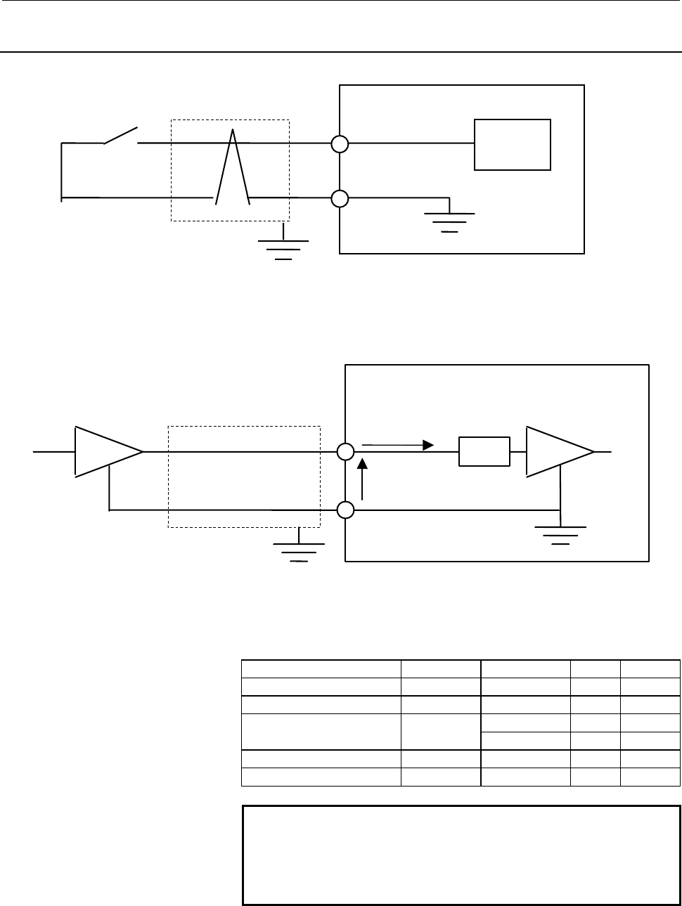
9.2.15.3 Skip signal interface
βi SVM
JA72
HDI (15)
0V (12,14,16)
Input signal specifications
- Circuit configuration
VH / VL
IiH / IiL
Driver
Shield
Filter
Receiver
β
i SVM
- Maximum absolute rating
Input voltage range Vin: -3.6 V to +13.6 V
- Input characteristics
Item Signal Specification Unit Remarks
High level input voltage VH 3.6-11.6 V
Low level input voltage VL 0-0.55 V
2 max MA Vin=5V
High level input current IiH
11 max MA Vin=10V
Low level input current IiL -8.0 max MA Vin=0V
Input signal pulse width 20 min µs
NOTE
The positive sign (+) of IiH/IiL indicates the
direction in which current flows into the receiver,
and the negative sign (-) indicates the direction in
which current flows out of the receiver.
Receiver
Contents Summary of Servo Amplifier Beta i Descriptions
- Page 1GE Fanuc Automation Europe Computer Numerical Controls Fanuc AC Servo Amplifiers βi Series Description Manual B-65322EN/02 TECHNOLOGY AND MORE
- Page 2Ȧ No part of this manual may be reproduced in any form. Ȧ All specifications and designs are subject to change without notice. In this manual we have tried as much as possible to describe all the various matters. However, we cannot describe all the matters which must not be done, or which cannot be
- Page 3B-65322EN/02 SAFETY PRECAUTIONS SAFETY PRECAUTIONS This "Safety Precautions" section describes the precautions which must be observed to ensure safety when using FANUC servo amplifiers (including spindle amplifiers). Users of any servo amplifier model are requested to read the "Safety Precautions" c
- Page 4SAFETY PRECAUTIONS B-65322EN/02 1.1 DEFINITION OF WARNING, CAUTION, AND NOTE This manual includes safety precautions for protecting the user and preventing damage to the machine. Precautions are classified into Warning and Caution according to their bearing on safety. Also, supplementary information
- Page 5B-65322EN/02 SAFETY PRECAUTIONS 1.2 WARNINGS AND CAUTIONS RELATING TO MOUNTING 1.2.1 Warning WARNING - Check the specification code of the amplifier. Check that the delivered amplifier is as originally ordered. - Mount a ground fault interrupter. To guard against fire and electric shock, fit the fac
- Page 6SAFETY PRECAUTIONS B-65322EN/02 WARNING - Close the amplifier cover after completing the wiring. Leaving the cover open presents a danger of electric shock. - Do not disassemble the amplifier. - Ensure that the cables used for the power supply lines and power lines are of the appropriate diameter an
- Page 7B-65322EN/02 SAFETY PRECAUTIONS 1.2.2 Caution CAUTION - Do not step or sit on the amplifier. Also, do not stack unpacked amplifiers on top of each other. - Use the amplifier in an appropriate environment. See the allowable ambient temperatures and other requirements, given in the this manual. - Prot
- Page 8SAFETY PRECAUTIONS B-65322EN/02 CAUTION - Check that the amplifier is securely mounted in the power magnetic cabinet. If any clearance is left between the power magnetic cabinet and the surface on which the amplifier is mounted, dust entering the gap may build up and prevent the normal operation of
- Page 9B-65322EN/02 SAFETY PRECAUTIONS 1.2.3 Note NOTE - Keep the nameplate clearly visible. - Keep the legend on the nameplate clearly visible. - After unpacking the amplifier, carefully check for any damage. - Mount the amplifier in a location where it can be easily accessed periodic inspection and daily
- Page 10SAFETY PRECAUTIONS B-65322EN/02 1.3 WARNINGS AND CAUTIONS RELATING TO A PILOT RUN 1.3.1 Warning WARNING - Before turning on the power, check that the cables connected to the power magnetic cabinet and amplifier, as well as the power lines and power supply lines, are securely connected. Also, check t
- Page 11B-65322EN/02 SAFETY PRECAUTIONS 1.3.2 Caution CAUTION - Note whether an alarm status relative to the amplifier is displayed at power-up or during operation. If an alarm is displayed, take appropriate action as explained in the maintenance manual. If the work to be done requires that the door of the
- Page 12SAFETY PRECAUTIONS B-65322EN/02 1.4 Warnings and Cautions Relating to Maintenance 1.4.1 Warning WARNING - Read the maintenance manual carefully and ensure that you are totally familiar with its contents. The maintenance manual describes daily maintenance and the procedures to be followed in the even
- Page 13B-65322EN/02 SAFETY PRECAUTIONS WARNING - Notes on replacing the battery of the absolute Pulsecoder Replace the battery only while the power is on. If the battery is replaced while the power is turned off, the stored absolute positioning data will be lost. Some βi series servo amplifier modules have
- Page 14SAFETY PRECAUTIONS B-65322EN/02 1.4.2 Caution CAUTION - Ensure that all required components are mounted. When replacing a component or PC board, check that all components, including the snubber capacitor, are correctly mounted. If the snubber capacitor is not mounted, for example, the IPM will be da
- Page 15B-65322EN/02 SAFETY PRECAUTIONS 1.4.3 Note NOTE - Ensure that the battery connector is correctly inserted. If the power is shut off while the battery connector is not connected correctly, the absolute position data for the machine will be lost. - Store the manuals in a safe place. The manuals should
- Page 16
- Page 17B-65322EN/02 TABLE OF CONTENTS TABLE OF CONTENTS SAFETY PRECAUTIONS............................................................................s-1 I. SVM 1 OVERVIEW ............................................................................................. 3 2 CONFIGURATION .......................
- Page 18TABLE OF CONTENTS B-65322EN/02 5.2.1 Specification...........................................................................................................28 5.2.2 How to Select a Transformer..................................................................................29 6 INSTALLATION CONDITI
- Page 19B-65322EN/02 TABLE OF CONTENTS 9.1.2 SVM1-40i and SVM1-80i ......................................................................................68 9.2 CONNECTOR LOCATION .......................................................................... 70 9.2.1 SVM1-4i and SVM1-20i ........................
- Page 20TABLE OF CONTENTS B-65322EN/02 3.5.1 AC Line Filter and Magnetic Contactor...............................................................108 3.5.2 AC Reactor ...........................................................................................................109 3.6 SPINDLE AXIS TYPES (#A AND
- Page 21B-65322EN/02 TABLE OF CONTENTS 9.3.1.2 Details of cable K6 .......................................................................................... 144 9.3.1.3 Details of cable K7 .......................................................................................... 145 9.3.1.4 Details of cabl
- Page 22TABLE OF CONTENTS B-65322EN/02 3.3.1 Selecting Circuit Breaker .....................................................................................191 3.3.2 Selecting Magnetic Contactor ..............................................................................191 3.3.3 Selecting AC Line Filter.
- Page 23B-65322EN/02 TABLE OF CONTENTS 8.3.3 Maintenance Area for the SVM1-80i ...................................................................205 9 TOTAL CONNECTION DIAGRAM...................................................... 206 9.1 CONNECTION DIAGRAM ..................................................
- Page 24TABLE OF CONTENTS B-65322EN/02 10 HEAT DISSIPATION ........................................................................... 239 APPENDIX A CONNECTING THE REACTOR AND LINE FILETER ........................ 243 A.1 OVERVIEW ............................................................................
- Page 25I. SV
- Page 26
- Page 27B-65322EN/02 SVM 1.OVERVIEW 1 OVERVIEW The βi SVM FSSB interface has the following features: (1) Because a power supply is incorporated, a compact system can be built for 1- or 2-axis machining. (2) One-axis AC servo system with excellent cost performance (3) The FSSB interface, which is the standar
- Page 282.CONFIGURATION SVM B-65322EN/02 2 CONFIGURATION -4-
- Page 29B-65322EN/02 SVM 2.CONFIGURATION 2.1 SVM1-4i AND SVM1-20i Fan unit Dummy connector for fan 4-A type, 20-A type βi βi Connector for fan SVM SVM 20A 4A FUSE FUSE Stabilized +24V etc power supply CXA19B CXA19A CXA19B CXA19A 24 VDC NC Optical cable COP10B COP10A COP10B COP10A 3-phase : 200 to 240 VAC 1-
- Page 302.CONFIGURATION SVM B-65322EN/02 2.2 SVM1-40i AND SVM1-80i 40-A type, 80-A type βi βi SVM SVM 80A 40A FUSE FUSE Stabilized +24V etc power supply CXA19B CXA19A CXA19B CXA19A 24 VDC NC Optical cable COP10B COP10A COP10B COP10A 3-phase 200 to 240 VAC Optical cable Circuit Magnetic AC line CZ4 CZ4 break
- Page 31B-65322EN/02 SVM 3.SPECIFICATIONS 3 SPECIFICATIONS -7-
- Page 323.SPECIFICATIONS SVM B-65322EN/02 3.1 SPECIFICATIONS Item SVM-4i SVM-20i SVM1-40i SVM1-80i Interface FSSB Unit drawing No. A06B-6130-H001 A06B-6130-H002 A06B-6130-H003 A06B-6130-H004 Power PC board drawing No. A20B-2101-0090 A20B-2101-0091 A16B-3200-0512 A16B-3200-0513 Control PC board drawing No. A
- Page 33B-65322EN/02 SVM 3.SPECIFICATIONS 3.3 SELECTING CIRCUIT BREAKER, MAGNETIC CONTACTOR, AND AC LINE FILTER 3.3.1 Selecting Circuit Breaker Select a circuit breaker based on the continuous current ratings of the individual motors listed below. When connecting more than one amplifier, determine the ratin
- Page 343.SPECIFICATIONS SVM B-65322EN/02 3.3.2 Selecting Magnetic Contactor Select a magnetic contactor according to the table, "Input current for continuous output rating". When connecting more than one amplifier, make a selection based on the sum of the continuous current ratings of the motors. Manufactu
- Page 35B-65322EN/02 SVM 3.SPECIFICATIONS 3.4 COOLING FAM MOTORS 3.4.1 Models Requiring Cooling Fan motors The combinations listed below require cooling fan motors. Ordering number Amplifier Combined motor A06B-6134-K002 SVM1-80i General 80-A class motors SVM1-20i α4/5000is Running on 3-phase β8/3000is 200-
- Page 363.SPECIFICATIONS SVM B-65322EN/02 3.5 DERATING Consider derating as shown below, according to ambient temperatures. SVM1-20i Output derating for single-phase input 1200 Motor output (W) 900 With fan 750 Without fan 500 0 0 35 45 55 Temperature (°C) SVM1-40i Output derating for 3-phase input 13.0 9.8
- Page 37B-65322EN/02 SVM 3.SPECIFICATIONS 3.6 SEPARATED REGENERATIVE DISCHARGE RESISTOR 3.6.1 When No Separated Regenerative Discharge Resistor Is Needed No separated regenerative discharge resistor is needed if the energy regenerated per regeneration cycle is not higher than the amount [J] of energy listed
- Page 383.SPECIFICATIONS SVM B-65322EN/02 - For vertical movement (a) SI unit system −1 Q = 1.047 × 10 ⋅ Th ⋅ Vm ⋅ ta [ J ] (Expression 2) Th: Upward torque that the motor applies at the time of downward rapid traverse [N⋅m] Vm: Motor speed at rapid traverse [min-1] ta : Rapid traverse acceleration/decelera
- Page 39B-65322EN/02 SVM 3.SPECIFICATIONS 3.6.2 When a Separated Regenerative Discharge Resistor Is Needed If the amount of energy regenerated per regeneration cycle exceeds the maximum amount of energy that a servo amplifier can handle, a DC link overvoltage alarm occurs. In this case, a separated regenera
- Page 403.SPECIFICATIONS SVM B-65322EN/02 - For vertical movement The amount of regenerative discharge (power [W]) when the operation duty for downward rapid traverse is D(%) (a) SI unit system −1 D w 2 = 1.047 × 10 ⋅ Th ⋅ Vm × [W ] (Expression 5) 100 Th: Upward torque that the motor applies at the time of
- Page 41B-65322EN/02 SVM 3.SPECIFICATIONS 3.6.3 When Amplifier Models SVM-40i and SVM-80i Are Used If the amount of regenerative discharge from a servo motor exceeds the regenerative discharge capacity of the regenerative discharge resistor incorporated in the corresponding servo amplifier, a separated rege
- Page 423.SPECIFICATIONS SVM B-65322EN/02 Set-up switch (for changing the DC alarm level) Switch setting (for the SVM1-40i and SVM1-80i) The SVM1-40i and SVM1-80i each have four switches on their front panel for protecting regenerative resistors. Be sure to set these switches to the positions that match the
- Page 43B-65322EN/02 SVM 3.SPECIFICATIONS Cautions for selecting a regenerative discharge resistor WARNING 1 Regenerative discharge resistors may become very hot (100 to 200 °C). Be careful not to touch them. 2 Before touching a regenerative discharge resistor, for example, for maintenance purposes, turn of
- Page 443.SPECIFICATIONS SVM B-65322EN/02 Installation and connection of A06B-6130-H401 To connector CZ7 To connector CXA20 WARNING 1 Regenerative discharge resistors may become very hot (100 to 200 °C). Be careful not to touch them. 2 Before touching a regenerative discharge resistor, for example, for main
- Page 45B-65322EN/02 SVM 3.SPECIFICATIONS Installation and connection of A06B-6130-H402 Front Side A Side B Installation direction Up * Spacer Wall ABCD A, D: To connector CZ7 B, C: To connector CXA20 Yamanashi 401-05 97 JAPAN made in JAPAN WARNING 1 Regenerative discharge resistors may become very hot (100
- Page 464.ORDERING INFORMATION SVM B-65322EN/02 4 ORDERING INFORMATION Refer to the order list (B-65321EN). - 22 -
- Page 47B-65322EN/02 SVM 5.POWER SUPPLY 5 POWER SUPPLY - 23 -
- Page 485.POWER SUPPLY SVM B-65322EN/02 5.1 INPUT POWER SUPPLY 5.1.1 Three-phase Input Power Supply for Motor Power - Nominal rated voltage: 200 to 240 VAC - Allowable voltage fluctuation: -15% to +10% - Frequency: 50/60 Hz - Allowable frequency fluctuation: ±2 Hz - Power supply impedance: Voltage fluctuati
- Page 49B-65322EN/02 SVM 5.POWER SUPPLY Power supply rating per amplifier FSSB interface 0.9A - External 24-VDC power supply specifications Recommended external 24-VDC power supply (stabilized power supply) specifications (UL1950 must be satisfied.) Output voltage +24V ±10% (21.6V to 26.4V) (Including rippl
- Page 505.POWER SUPPLY SVM B-65322EN/02 (1) Timing chart Momentary Momentary disconnection disconnection (-100%) (-50%) AC input voltage 10mS 20mS 26.4V Output voltage 21.6V Abrupt change in load Output current 0A Figure Example of ripple voltage and noise due to switching power supply 26.4V Noise To be wit
- Page 51B-65322EN/02 SVM 5.POWER SUPPLY - Circuit configuration The circuit configuration shown in <1> and <2> below are not permitted. Prohibited <1> Circuit examples in which the output voltage cannot be held at the time of momentary disconnection (the voltage level lowers below 21.6 V) Example 1 Rectifie
- Page 525.POWER SUPPLY SVM B-65322EN/02 5.2 POWER TRANSFORMER FOR EXPORTS Use power transformer for an export when this servo amplifier unit is used at a site where the line voltage is other than 200 to 240 VAC. 5.2.1 Specification Table 5.2.1 Specification of power transformer Ordering drawing number A80L-
- Page 53B-65322EN/02 SVM 5.POWER SUPPLY 5.2.2 How to Select a Transformer Select a transformer according to the load condition and the model of the motor for which the transformer is used. Each transformer has secondary winding taps for three amplifiers so that it can be connected to two or three amplifiers
- Page 546.INSTALLATION CONDITIONS AND NOTES SVM B-65322EN/02 6 INSTALLATION CONDITIONS AND NOTES - 30 -
- Page 55B-65322EN/02 SVM 6.INSTALLATION CONDITIONS AND NOTES 6.1 ENVIRONMENTAL CONDITIONS Install a βi setting servo amplifier in a completely closed cabinet so that the environment conditions indicated below can be satisfied. (1) Ambient Temperature Ambient temperature 0 to 55°C (operating) -20 to 60°C (st
- Page 566.INSTALLATION CONDITIONS AND NOTES SVM B-65322EN/02 6.2 SELECTING A GROUND-FAULT CIRCUIT INTERRUPTER Because the servo amplifier βi series uses the PWM inverter system by transistors to drive a motor, high frequency leakage current flows via the motor winding, power cable, and amplifier floating ca
- Page 57B-65322EN/02 SVM 6.INSTALLATION CONDITIONS AND NOTES 6.3 NOISE PROTECTION 6.3.1 Separation of Signal Lines If a power cable and signal cable run close to each other, noise can be induced. So, ensure that a power cable is separated from a signal cable. When a power cable and signal line cannot be sep
- Page 586.INSTALLATION CONDITIONS AND NOTES SVM B-65322EN/02 6.3.2 Grounding A CNC machine tool has three separate ground systems: (1) Signal ground (SG) system The signal ground (SG) system provides the reference potential (0V) for the electrical signal system. (2) Frame ground (FG) system The frame ground
- Page 59B-65322EN/02 SVM 6.INSTALLATION CONDITIONS AND NOTES 6.3.3 Noise Suppressor The AC/DC solenoid and relay are used in the power magnetics cabinet. A high pulse voltage is caused by coil inductance when these devices are turned on or off. This pulse voltage induced through the cable causes the electro
- Page 606.INSTALLATION CONDITIONS AND NOTES SVM B-65322EN/02 6.3.4 Cable Clamp and Shield Processing - Shield terminal processing Process the terminal of the shield cover of a signal line according to Chapter 10, "DETAILS OF CABLE CONNECTION". - Shield clamping The amplifier cables that require shielding sh
- Page 61B-65322EN/02 SVM 6.INSTALLATION CONDITIONS AND NOTES Machine side installation board Control unit Ground plate Metal fittings for clamp Shield cover Fig.6.3.4(b) Cable clamp (2) Prepare ground plate like the following figure. Ground terminal (grounded) Hole for securing metal fitting clamp Mount scr
- Page 626.INSTALLATION CONDITIONS AND NOTES SVM B-65322EN/02 For the ground plate, use a metal plate of 2 mm or thicker, which surface is plated with nickel. Ground plate Fig.6.3.4(d) Ground plate holes (Reference) Outer drawings of metal fittings for clamp. Max. 55mm Fig.6.3.4(e) Outer drawings of metal fi
- Page 63B-65322EN/02 SVM 6.INSTALLATION CONDITIONS AND NOTES 6.4 INSTALLING LIGHTNING SURGE ABSORBERS At the power input of the power magnetics cabinet, install a surge absorber between the power lines and between each power line and a ground to protect the unit from a voltage surge caused by lightning. How
- Page 646.INSTALLATION CONDITIONS AND NOTES SVM B-65322EN/02 (2) Surge absorber for single-phase input When using an integrated lightning surge absorber between the power lines and between each power line and a ground Lightning surge absorber between power lines and between each line and ground (R.C.M-601BU
- Page 65B-65322EN/02 SVM 6.INSTALLATION CONDITIONS AND NOTES (3) Surge absorber for three-phase input WARNING 1 Make the wires shown with thick line in the above diagram as short as possible in order to increase the effect of the lightning surge absorber. Wire Cross section : At least 2mm2 Length : Keep the
- Page 667.PROTECTIVE GROUNDING SVM B-65322EN/02 7 PROTECTIVE GROUNDING - 42 -
- Page 67B-65322EN/02 SVM 7.PROTECTIVE GROUNDING 7.1 SVM1-4i and SVM1-20i (FSSB Interface) Servo unit Servo unit (Front view) (Side view) Air out Air in To be as short as possible To other ground plates Distribution panel in cabinet Ground plate Ground plate Connected to cabinet External distribution panel C
- Page 687.PROTECTIVE GROUNDING SVM B-65322EN/02 7.2 SVM1-40i and SVM1-80i (FSSB Interface) Clamp shield Inlet External shielded cable To be as short as possible Ground plate To system ground - 44 -
- Page 69B-65322EN/02 SVM 8.EXTERNAL DIMENSIONS / PANEL CUT-OUT DRAWINGS / MAINTENANCE AREA 8 EXTERNAL DIMENSIONS / PANEL CUT-OUT DRAWINGS / MAINTENANCE AREA - 45 -
- Page 708.EXTERNAL DIMENSIONS / PANEL CUT-OUT DRAWINGS / MAINTENANCE AREA SVM B-65322EN/02 8.1 EXTERNAL DIMENSIONS 8.1.1 External Dimensions of SVM1-4i and SVM1-20i Amplifier alone Weight : 1.2kg Amplifier with a regenerative resistor, fan motor, and battery attached Weight : 1.3kg - 46 -
- Page 71B-65322EN/02 SVM 8.EXTERNAL DIMENSIONS / PANEL CUT-OUT DRAWINGS / MAINTENANCE AREA 8.1.2 External Dimensions of SVM1-40i and SVM1-80i Yamanashi 401-0597 JAPAN 380 360 30 172 100 max. 60 Weight : 3.9kg - 47 -
- Page 728.EXTERNAL DIMENSIONS / PANEL CUT-OUT DRAWINGS / MAINTENANCE AREA SVM B-65322EN/02 8.1.3 External Dimensions of Fan Unit (A06B-6134-K003) 6.5 62 60 17.5 max. 60 60 Yamanashi 401-0 597 JAPA N m ade in JAPAN 75 - 48 -
- Page 73B-65322EN/02 SVM 8.EXTERNAL DIMENSIONS / PANEL CUT-OUT DRAWINGS / MAINTENANCE AREA 8.1.4 External Dimensions of Fan Unit (A06B-6134-K002) - 49 -
- Page 748.EXTERNAL DIMENSIONS / PANEL CUT-OUT DRAWINGS / MAINTENANCE AREA SVM B-65322EN/02 8.1.5 Discharge Resistor A06B-6130-H401 Weight: 0.07 kg A06B-6130-H402 Weight: 0.5 kg - 50 -
- Page 75B-65322EN/02 SVM 8.EXTERNAL DIMENSIONS / PANEL CUT-OUT DRAWINGS / MAINTENANCE AREA A06B-6089-H500 - 51 -
- Page 768.EXTERNAL DIMENSIONS / PANEL CUT-OUT DRAWINGS / MAINTENANCE AREA SVM B-65322EN/02 A06B-6089-H713 to H714 (Pay attention to high temperature) Up Installation direction Label Packing Packing Drawing No. Weight - 52 -
- Page 77B-65322EN/02 SVM 8.EXTERNAL DIMENSIONS / PANEL CUT-OUT DRAWINGS / MAINTENANCE AREA 8.1.6 AC Line Filter A81L-0001-0083#3C A81L-0001-0101#C - 53 -
- Page 788.EXTERNAL DIMENSIONS / PANEL CUT-OUT DRAWINGS / MAINTENANCE AREA SVM B-65322EN/02 A81L-0001-0102 - 54 -
- Page 79B-65322EN/02 SVM 8.EXTERNAL DIMENSIONS / PANEL CUT-OUT DRAWINGS / MAINTENANCE AREA 8.1.7 Transformer for Exports Drawing No. A80L-0022-0005 A80L-0024-0006 A80L-0026-0003 A80L-0028-0001 Type (name) SAE SBE SCE SDE Weight 21 kg 27 kg 36 kg 42 kg hl* (transformer height) 217 mm max 217 mm max 247 mm ma
- Page 808.EXTERNAL DIMENSIONS / PANEL CUT-OUT DRAWINGS / MAINTENANCE AREA SVM B-65322EN/02 8.1.9 Lightning Surge Absorbers (a) A06B-6077-K142 Connection diagram (1) Between power lines: RAV-781BYZ-2 Connection diagram (2) Between each power line and ground: RAV-781BXZ-4 Withstanding Specification Rated volt
- Page 81B-65322EN/02 SVM 8.EXTERNAL DIMENSIONS / PANEL CUT-OUT DRAWINGS / MAINTENANCE AREA (b) A06B-6077-K144 Circuit diagram Maximum surge Rated AC discharge Withstanding Withstanding Specification Clamp voltage discharge start voltage start voltage surge current surge voltage voltage 560 VAC 2000V 2500A 2
- Page 828.EXTERNAL DIMENSIONS / PANEL CUT-OUT DRAWINGS / MAINTENANCE AREA SVM B-65322EN/02 8.2 PANEL CUT-OUT DRAWINGS 8.2.1 SVM1-4i and SVM1-20i - 58 -
- Page 83B-65322EN/02 SVM 8.EXTERNAL DIMENSIONS / PANEL CUT-OUT DRAWINGS / MAINTENANCE AREA 8.2.2 SVM1-40i and SVM1-80i NOTE Attach the accompanying gasket around the panel cut-out to prevent oil and dust from getting into it. Reinforce the right and left sides of the panel cut-out in the power magnetics cab
- Page 848.EXTERNAL DIMENSIONS / PANEL CUT-OUT DRAWINGS / MAINTENANCE AREA SVM B-65322EN/02 8.2.3 Discharge Resistor A06B-6089-H500 CAUTION Attach the packing (acrylonitrile-butadiene rubber, NBR (soft type)) to prevent oil and dust from getting into the resistor. - 60 -
- Page 85B-65322EN/02 SVM 8.EXTERNAL DIMENSIONS / PANEL CUT-OUT DRAWINGS / MAINTENANCE AREA A06B-6089-H713 to H714 Panel cut-out Packing (supplied) Panel cut-out CAUTION Attach the packing (acrylonitrile-butadiene rubber, NBR (soft type)) to prevent oil and dust from getting into the resistor. - 61 -
- Page 868.EXTERNAL DIMENSIONS / PANEL CUT-OUT DRAWINGS / MAINTENANCE AREA SVM B-65322EN/02 8.3 MAINTENANCE AREA 8.3.1 Maintenance Area for the SVM1-4i and SVM1-20i - 62 -
- Page 87B-65322EN/02 SVM 8.EXTERNAL DIMENSIONS / PANEL CUT-OUT DRAWINGS / MAINTENANCE AREA 8.3.2 Maintenance Area for the SVM1-40i and SVM1-80i When no cooling fan AC motor (A06B-6134-K002) is used to cool the heat sink - 63 -
- Page 888.EXTERNAL DIMENSIONS / PANEL CUT-OUT DRAWINGS / MAINTENANCE AREA SVM B-65322EN/02 When the cooling fan AC motor (A06B-6134-K002) is used to cool the heat sink - 64 -
- Page 89B-65322EN/02 SVM 9.TOTAL CONNECTION DIAGRAM 9 TOTAL CONNECTION DIAGRAM - 65 -
- Page 909.TOTAL CONNECTION DIAGRAM SVM B-65322EN/02 9.1 CONNECTION DIAGRAM 9.1.1 SVM1-4i and SVM1-20i Dummy connector for fan 4-A type, 20-A type Fan unit Connector for βi βi fan SVM SVM 20A 4A FUSE FUSE Stabilized K11 K6 power supply CXA19B CXA19A CXA19B CXA19A 24 VDC NC Optical cable COP10B COP10A COP10B
- Page 91B-65322EN/02 SVM 9.TOTAL CONNECTION DIAGRAM NOTE 1 Always install the circuit breakers, magnetic contactor, and AC line filter. 2 To protect the equipment from lightning surge voltages, install a lightning surge absorber across each pair of power lines and across each power line and the grounding li
- Page 929.TOTAL CONNECTION DIAGRAM SVM B-65322EN/02 9.1.2 SVM1-40i and SVM1-80i 40-A type, 80-A type βi βi SVM SVM 80A 40A FUSE FUSE Stabilized K11 CXA19B CXA19A K6 CXA19B CXA19A power supply 24 VDC NC Optical cable COP10B COP10A COP10B COP10A 3-phase : 200 to 240VAC Optical cable Circuit Magnetic AC CZ4 CZ
- Page 93B-65322EN/02 SVM 9.TOTAL CONNECTION DIAGRAM WARNING Defects, such as a loose screw and an incorrectly inserted connector, can lead to a motor malfunction, excessive heat generation, and a ground fault. Exercise adequate care in installing servo amplifiers. A loose screw (or, if a connector is used,
- Page 949.TOTAL CONNECTION DIAGRAM SVM B-65322EN/02 9.2 CONNECTOR LOCATION 9.2.1 SVM1-4i and SVM1-20i No. Name Remarks 1 DC link charge LED CZ7-1 (1) 2 Main power input connector CZ7-2 3 CZ7-3 Discharge register connector (8)(9) CZ7-4 4 CZ7-5 Motor power connector CZ7-6 (10) Connector for main power MCC 5 C
- Page 95B-65322EN/02 SVM 9.TOTAL CONNECTION DIAGRAM 9.2.2 SVM1-40i and SVM1-80i No. Name Remarks 1 DC link charge LED Connector for main power MCC 2 CX29 control signal 3 CX30 ESP signal connection connector Regenerative resistor connector (for (9) 4 CXA20 (1) Yamanashi 401-0597 JAPAN alarms) Setting switch
- Page 969.TOTAL CONNECTION DIAGRAM SVM B-65322EN/02 9.2.3 Connection Tools The ordering specification drawing numbers of connection tools for connectors when the tools are purchased from FANUC are listed below. You may also purchase these tools directly from the manufacturer. Connectors manufactured by Tyco
- Page 97B-65322EN/02 SVM 9.TOTAL CONNECTION DIAGRAM 9.2.4 Details of Cable K1 9.2.4.1 Servo motor αi, αis series, Servo motor βis series (β0.4/5000is to β22/2000is) Shield SVM Servo motor (5) RD (6) (6) *RD (5) (9, 20) 5V (8, 9) (12, 14) 0V (7, 10) (7) 6V (4) Drain wire (16) FG (3) 20-pin half-pitch connect
- Page 989.TOTAL CONNECTION DIAGRAM SVM B-65322EN/02 NOTE 1 In case that the cable is prepared by MTB, total resistance of 5V and 0V must be less than 2Ω. 2 Pulsecoder side connector can accept maximum 0.5mm2 (wire construction 20/0.18 or 104/0.08, insulation outer diameter φ1.5 or less) wire and sheath diam
- Page 99B-65322EN/02 SVM 9.TOTAL CONNECTION DIAGRAM 9.2.4.2 Servo motor βis series (β0.2/5000is, β0.3/5000is) Shield SVM Servo motor (1) SD (A4) (2) *SD (B4) (5) REQ (A3) (6) *REQ (B3) (9, 20) 5V (A2, B2) (12, 14) 0V (A1, B1) (7) 6V (A5) (16) Drain wire FG (B6) 20-pin half-pitch connector Housing : 1-131811
- Page 1009.TOTAL CONNECTION DIAGRAM SVM B-65322EN/02 NOTE 1 The ground plate to which the shield is connected must be placed as close as possible to the servo amplifier so that distance between the ground plate and the servo amplifier becomes shortest. 2 In case that the cable is prepared by the user, the to
- Page 101B-65322EN/02 SVM 9.TOTAL CONNECTION DIAGRAM 9.2.5 Details of Cable K2 The following items related to servo amplifier input cables are explained below in the stated order. (1) Details of connectors (2) Selecting input cables (general) (3) Details of input cables 9.2.5.1 Details of connectors (a) SVM1
- Page 1029.TOTAL CONNECTION DIAGRAM SVM B-65322EN/02 [Receptacle contact] Two receptacle contact types are available, so as to support different conductor diameters. Be sure to select the receptacle contact that matches the servo axis you use. Conductor Conductor Rectangle contact Insulation outer Manual too
- Page 103B-65322EN/02 SVM 9.TOTAL CONNECTION DIAGRAM [Connector and tool ordering information] Connectors (including housings and contacts) and tools can be purchased directly from Tyco Electronics AMP. They can be ordered as options also from FANUC as listed below. Ordering number Description Housing : XX k
- Page 1049.TOTAL CONNECTION DIAGRAM SVM B-65322EN/02 9.2.5.2 Selecting cables (general) Select the cable specification by considering the following conditions for use: (1) Motor current rating or current needed in use on a real machine (2) Cable type (heat resistance temperature, etc.) (3) Environment in whi
- Page 105B-65322EN/02 SVM 9.TOTAL CONNECTION DIAGRAM 9.2.5.3 Details of input cables Select cables by taking the following conditions for use into account. [Example combinations of input cables for servo motors running with continuous-rating output (reference only)] Continuous Continuous [Example 1.] [Exampl
- Page 1069.TOTAL CONNECTION DIAGRAM SVM B-65322EN/02 9.2.6 Details of Cable K3 The following items related to servo motor/amplifier power cables are explained below in the stated order. (1) Details of connectors (2) Selecting power cables (general) (3) Power cable for servo motor 9.2.6.1 Details of connector
- Page 107B-65322EN/02 SVM 9.TOTAL CONNECTION DIAGRAM (b) SVM1-40i, SVM1-80i βi SVM Motor Receptacle housing CZ5 B1 U U A1 V V B2 W W A2 GND(Body) [Receptacle housing] Use the following receptacle housing. Manufacturer-defined Specification of the Manufacture model key 2-917807-2 YY Tyco Electronics AMP [Rece
- Page 1089.TOTAL CONNECTION DIAGRAM SVM B-65322EN/02 9.2.6.3 Power cable for servo motor A servo motor power cable assembly consists of: (a) Power cable (b) Motor-side connector (a) Power cable Examples of combining a servo motor and power cable are described below according to Subsection 5.2.4.2, “Selecting
- Page 109B-65322EN/02 SVM 9.TOTAL CONNECTION DIAGRAM 9.2.7 Details of Cables K4 and K5 9.2.7.1 SVM1-4i and SVM1-20i When a regenerative discharge resistor is used The following regenerative discharge resistor models are available. The following housing and contact are A06B-6130-H401 connected to the resistor
- Page 1109.TOTAL CONNECTION DIAGRAM SVM B-65322EN/02 When no regenerative discharge resistor is used βi SVM CZ7 DCP Keep these pins unconnected. (Do not install a jumper between the pins.) DCC CXA20 1 Install a jumper between the pins. 2 D-2000 series Housing : 1-1318120-3 Contact : 1318107-1 Manufacture : T
- Page 111B-65322EN/02 SVM 9.TOTAL CONNECTION DIAGRAM 9.2.7.2 SVM1-40i and SVM1-80i When a separated regenerative discharge resistor is used βi SVM Cable specification: Two-conductor polyvinyl heavy-duty power cable (JIS C3312), Conductor size of 3.5 mm2, Crimp terminal: 5.5-4 Separated regenerative discharge
- Page 1129.TOTAL CONNECTION DIAGRAM SVM B-65322EN/02 When a built-in regenerative discharge resistor is used βi SVM CZ6 A1 Install a jumper between the pins. RC A2 Cable specification: RI Two-conductor polyvinyl heavy-duty power cable (JIS C3312), Conductor size of 3.5 mm2, Crimp terminal: 5.5-4 D-5000 serie
- Page 113B-65322EN/02 SVM 9.TOTAL CONNECTION DIAGRAM 9.2.8 Details of Cable K6 βi SVM βi SVM CXA19B-A1 (24V) CXA19A –A1 (24V) CXA19B-B1 (24V) CXA19A-B1 (24V) CXA19B-A2 (0V) CXA19A –A2 (0V) CXA19B-B2 (0V) CXA19A-B2 (0V) CXA19B-A3 (ESP) CXA19A –A3 (ESP) WARNING CXA19B-B3 (BAT) CXA19A-B3 (BAT) WARNING D-2000 se
- Page 1149.TOTAL CONNECTION DIAGRAM SVM B-65322EN/02 9.2.9 Details of Cable K7 βi SVM MCC 1 CX29 Coil Spark killer Internal contact 3 External power supply (Use an appropriate power supply for the coil voltage the customer uses.) D-2000 series Housing : 3-1318130-3 Contact : 1318107-1 Applicable wire: 0.3 to
- Page 115B-65322EN/02 SVM 9.TOTAL CONNECTION DIAGRAM 9.2.10 Details of Cable K8 βi SVM CX30 24V 1 3 Receiver *ESP circuit D-2000 series Housing : 2-1318120-3 Contact : 1318107-1 Applicable wire: 0.3 to 0.85mm2 Manufacture : Tyco Electronics AMP For connection tools, see Subsection 9.2.3. (1) When the contact
- Page 1169.TOTAL CONNECTION DIAGRAM SVM B-65322EN/02 Emergency stop signal (*ESP) block diagram CXA19A-A3 Control RV LSI βiSVM for 1st axis CX30-3 24V R 0V CX30-1 CXA19A-A3 CXA19B-A3 Control RV LSI CX30-3 βiSVM for 2nd axis WARNING 24V R 0V CX30-1 CXA19A-A3 Control RV LSI WARNING CX30-3 βiSVM for 3rd axis 24
- Page 117B-65322EN/02 SVM 9.TOTAL CONNECTION DIAGRAM 9.2.11 Details of Cable K9 Battery case βi SVM A06B-6050-K060 CXA19A Battery A06B-6050-K061 24V 24V 0V A2 0V 0V ESP B3 BAT 6V D-2000 series Crimp terminal : 1.25-2 Housing : 1-1318119-3 Applicable wire : 0.3 to 0.85mm2 Contact : 1318107-1 Applicable wire :
- Page 1189.TOTAL CONNECTION DIAGRAM SVM B-65322EN/02 9.2.12 Details of Cable K10 (1) Incorporating built-in batteries in each SVM (For SVM1-4i or SVM1-20i) SVM SVM CX5X CX5X Battery case Battery case A06B-6093-K002 A06B-6093-K002 Battery Battery A06B-6093-K001 A06B-6093-K001 - Using the built-in battery (A06
- Page 119B-65322EN/02 SVM 9.TOTAL CONNECTION DIAGRAM (2) Incorporating built-in batteries in each SVM (For SVM1-40i or SVM1-80i) SVM SVM Battery case Battery case A06B-6093-K002 A06B-6093-K002 Battery Battery A06B-6093-K001 A06B-6093-K001 CX5X CX5X - Using the built-in battery (A06B-6093-K001) requires the b
- Page 1209.TOTAL CONNECTION DIAGRAM SVM B-65322EN/02 9.2.13 Details of Cable K11 βi SVM Stabilized power supply (24VDC) CXA19 B A1 24V 24V 24V A2 0V 0V 0V ESP D-2000 series Housing : 1-1318119-3 BAT Contact : 1318107-1 Applicable wire : 0.3 to 0.85mm2 Manufacture : Tyco Electronics AMP Up to four units can b
- Page 121B-65322EN/02 SVM 9.TOTAL CONNECTION DIAGRAM 9.3 HANDLING OF EXTERNAL MAGNETIC CONTACTORS This section explains how to handle external magnetic contactors when FSSB interface SVMs and I/O Link interface SVMs are used together. 1 Multiple FSSB interface SVMs can share an external magnetic contactor. D
- Page 12210.HEAT DISSIPATION SVM B-65322EN/02 10 HEAT DISSIPATION The amount of heat dissipation depends on the SVM model and the current that flows through the servo motor. For the current that flows through a servo motor, reference the continuous rated current of each servo motor. (For the continuous rated
- Page 123II. SVP
- Page 124
- Page 125B-65322EN/02 SVPM 1.OVERVIEW 1 OVERVIEW The βi series SVPM has the following features: (1) Because a power supply is incorporated, a system with two or three servo axes and one spindle can be built easily. (2) Multi-axis AC servo amplifier with excellent cost performance (3) This unit is designed in
- Page 1262.CONFIGURATION SVPM B-65322EN/02 2 CONFIGURATION Configuration of βi series servo amplifier SVPM Fan unit Fan unit SVPM JF1 Servo Motor Pulse Coder I/F JF2 Servo Motor JF3 Servo Motor JX6 CX3 JY1 LM, SM, OVR JA7A CNC Emergency stop CX4 Spindle I/F JA7B CNC CXA2C 24V power supply JYA2 Spindle Motor
- Page 127B-65322EN/02 SVPM 3.SPECIFICATIONS 3 SPECIFICATIONS - 103 -
- Page 1283.SPECIFICATIONS SVPM B-65322EN/02 3.1 SPECIFICATIONS Two-axis type (SVPM2) SVPM2-5.5i SVPM2-5.5i SVPM2-11i SVPM2-11i SVPM2-15i SVPM2-15i Item (TypeA) (TypeC) (TypeA) (TypeC) (TypeA) (TypeC) Unit specification A06B-6134-H201#A A06B-6134-H201#C A06B-6134-H202#A A06B-6134-H202#C A06B-6134-H203#A A06B-
- Page 129B-65322EN/02 SVPM 3.SPECIFICATIONS Three-axis type (SVPM3) SVPM3-5.5i SVPM3-5.5i SVPM3-11i SVPM3-11i SVPM3-15i SVPM3-15i Item (TypeA) (TypeC) (TypeA) (TypeC) (TypeA) (TypeC) Unit specification A06B-6134-H301#A A06B-6134-H301#C A06B-6134-H302#A A06B-6134-H302#C A06B-6134-H303#A A06B-6134-H303#C Power
- Page 1303.SPECIFICATIONS SVPM B-65322EN/02 3.2 COOLING FAN MOTOR Install a cooling fan motor listed below. Otherwise, make arrangements so that the required air flow can be obtained. Ordering number Optional fan Required air flow SVPM2-5.5i SVPM3-5.5i A06B-6134-K001 A06B-6134-H201#* A06B-6134-H301#* One uni
- Page 131B-65322EN/02 SVPM 3.SPECIFICATIONS 3.4 APPLICABLE MOTORS Spindle Motor Servo Motor β3/10000i β6/10000i β8/8000i β12/7000i β2/4000is β4/4000is β8/3000is β12/3000is β22/2000is Spindle O SVPM2-5.5i Servo L axis O O O A06B-6134-H201* Servo M axis O O O Spindle ** O O SVPM2-11i Servo L axis O O O A06B-61
- Page 1323.SPECIFICATIONS SVPM B-65322EN/02 3.5 CIRCUIT BREAKER, MAGNETIC CONTACTOR, AND AC REACTOR 3.5.1 AC Line Filter and Magnetic Contactor The ratings of the circuit breakers and magnetic contactor are determined by the specifications of the power supply module used. The ordering specification drawing n
- Page 133B-65322EN/02 SVPM 3.SPECIFICATIONS - Ordering specification drawing number of circuit breaker 1 Ordering Circuit breaker Circuit breaker cover Type Applicable model specification specification specification drawing No. SVPM*-5.5i A06B-6077-K102 Fuji Electric, EA103B/50 Fuji Electric, BZ-TB20B-3 (*:
- Page 1343.SPECIFICATIONS SVPM B-65322EN/02 3.6 SPINDLE AXIS TYPES (#A AND #C) AND APPLICABLE SENSORS Two models (#A and #C) are available for each sensor for spindles. The following table lists combinations of applicable sensors and functions. Configuration Remarks 1 2 3 4 5 6 Ordering number #A (TYPE A) A0
- Page 135B-65322EN/02 SVPM 3.SPECIFICATIONS 3.7 DERATING Derating Consider derating as shown below, according to ambient temperatures. Target models: All SVPM models 15 min. Available Operating Time 10 min. 5 min. 0 0 10 20 30 40 50 60 °C Ambient temperature - 111 -
- Page 1364.ORDERING INFORMATION SVPM B-65322EN/02 4 ORDERING INFORMATION Refer to the order list (B-65321EN). - 112 -
- Page 137B-65322EN/02 SVPM 5.POWER SUPPLY 5 POWER SUPPLY - 113 -
- Page 1385.POWER SUPPLY SVPM B-65322EN/02 5.1 INPUT POWER SUPPLY 5.1.1 Three-phase Input Power Supply for Motor Power - Nominal rated voltage: 200 to 240 VAC - Allowable voltage fluctuation: -15% to +10% - Frequency: 50/60 Hz - Allowable frequency fluctuation: ±2 Hz - Power supply impedance: Voltage fluctuat
- Page 139B-65322EN/02 SVPM 5.POWER SUPPLY 5.1.2 Single-phase Input for Control Power Be sure to use a stabilized power supply as the 24-V power supply for amplifiers. The 24-V power supply for motor brakes cannot be shared. - Nominal rated voltage: 24VDC - Allowable voltage fluctuation: ±10%(including moment
- Page 1405.POWER SUPPLY SVPM B-65322EN/02 5.2 POWER TRANSFORMER FOR EXPORTS When a SVPM of the 200V input series is used in an area where the input voltage is not within the range of 200 to 230VAC, a power transformer is required. The ordering drawing numbers and specifications of power transformers manufact
- Page 141B-65322EN/02 SVPM 5.POWER SUPPLY - Specifications of power transformers manufactured by FANUC Power transformer for SVPM Model SVPM*-5.5i SVPM*-11i SVPM*-15i Item Ordering drawing A06B-6052-J001 A06B-6044-J006 A06B-6044-J007 number FANUC drawing A80L-0001-0496 A80L-0001-0313 A80L-0001-0314 number Ra
- Page 1425.POWER SUPPLY SVPM B-65322EN/02 - Connecting a power transformer Power transformers must be set according to the supply voltage used. (a) Connection points of power transformers for SVPM*-5.5i, SVPM*-11i, and SVPM*-15i Supply Connection points at the primary Remarks voltage 380VAC R - R1, S - S1, T
- Page 143B-65322EN/02 SVPM 6.INSTALLATION CONDITIONS AND NOTES 6 INSTALLATION CONDITIONS AND NOTES - 119 -
- Page 1446.INSTALLATION CONDITIONS AND NOTES SVPM B-65322EN/02 6.1 ENVIRONMENTAL CONDITIONS See Chapter 6 in Part I “SVM”. 6.2 Selecting a Ground-Fault Circuit Interrupter See Chapter 6 in Part I “SVM”. 6.3 NOISE PROTECTION See Chapter 6 in Part I “SVM”. - 120 -
- Page 145B-65322EN/02 SVPM 6.INSTALLATION CONDITIONS AND NOTES 6.4 INSTALLING LIGHTNING SURGE ABSORBERS At the power input of the power magnetics cabinet, install a surge absorber between the power lines and between each power line and a ground to protect the unit from a voltage surge caused by lightning. Ho
- Page 1466.INSTALLATION CONDITIONS AND NOTES SVPM B-65322EN/02 WARNING 1 Make the wires shown with thick line in the above diagram as short as possible in order to increase the effect of the lightning surge absorber. Wire Cross section : At least 2mm2 Length : Keep the total wire length (a+b) to within 2m,wh
- Page 147B-65322EN/02 SVPM 7.PROTECTIVE GROUNDING 7 PROTECTIVE GROUNDING L-shaped metal plate (TB2 grounding terminal) Flange tapped hole Use short cable. Ground plate of cabinet To system ground - 123 -
- Page 1488.EXTERNAL DIMENSIONS / PANEL CUT-OUT DRAWINGS / MAINTENANCE AREA SVPM B-65322EN/02 8 EXTERNAL DIMENSIONS / PANEL CUT-OUT DRAWINGS / MAINTENANCE AREA - 124 -
- Page 149B-65322EN/02 SVPM 8.EXTERNAL DIMENSIONS / PANEL CUT-OUT DRAWINGS / MAINTENANCE AREA 8.1 EXTERNAL DIMENSIONS 8.1.1 External Dimensions of SVPM 380 mm 260 mm 172 mm 92.5 mm max. Weight : 14.8 kg 8.1.2 External Dimensions of Fan Unit (A06B-6134-K001) 120 mm 200VAC IN Note) ( 15 mm) 85 mm ( 55 mm) ( 15
- Page 1508.EXTERNAL DIMENSIONS / PANEL CUT-OUT DRAWINGS / MAINTENANCE AREA SVPM B-65322EN/02 8.1.3 AC Reactor Unit Max.B H D A F M- C E G K Applicable model A B C D E F G H K M- For SVPM-5.5i, 11i 135 155 82 50 65 89 48 135 5 M5 For SVPM-15i 135 155 108 42 95 84 66 135 7.2 M5 - 126 -
- Page 151B-65322EN/02 SVPM 8.EXTERNAL DIMENSIONS / PANEL CUT-OUT DRAWINGS / MAINTENANCE AREA 8.1.4 Power Transformer (a) For SVPM-5.5i (A06B-6052-J001) Terminal M4 Outline Drawing of Power Transformer with no Cover Outline Drawing of Power Transformer with Cover NOTE The four side panels are all meshed, whil
- Page 1528.EXTERNAL DIMENSIONS / PANEL CUT-OUT DRAWINGS / MAINTENANCE AREA SVPM B-65322EN/02 (b) For SVPM-11i (A06B-6044-J006) Terminal M6 Outline Drawing of Power Transformer with no Cover Outline Drawing of Power Transformer with Cover NOTE The four side panels are all meshed, while the top is a solid plat
- Page 153B-65322EN/02 SVPM 8.EXTERNAL DIMENSIONS / PANEL CUT-OUT DRAWINGS / MAINTENANCE AREA (c) For SVPM-15i (A06B-6044-J007) Terminal M6 Outline Drawing of Power Transformer with no Cover Outline Drawing of Power Transformer with Cover NOTE The four side panels are all meshed, while the top is a solid plat
- Page 1548.EXTERNAL DIMENSIONS / PANEL CUT-OUT DRAWINGS / MAINTENANCE AREA SVPM B-65322EN/02 8.1.5 Circuit Breaker Ordering A B C D E M1- F G H I J K L M2- N Mounting drawing number A06B-6077-K102 (For SVPM*-5.5i) 2 A06B-6077-K103 75 50 190 115 130 M8 17 80 56 49 φ8 φ5 110 M4 25 positions (For SVPM*-11i) (1)
- Page 155B-65322EN/02 SVPM 8.EXTERNAL DIMENSIONS / PANEL CUT-OUT DRAWINGS / MAINTENANCE AREA 8.1.6 Magnetic Contactors (a) A06B-6077-K122, A06B-6077-K123 (Dimensions with cover for protecting live parts) Coil terminal M3.5 Main terminal M5 (Dimensions with cover for protecting live parts) Auxiliary terminal
- Page 1568.EXTERNAL DIMENSIONS / PANEL CUT-OUT DRAWINGS / MAINTENANCE AREA SVPM B-65322EN/02 A06B-6077-K124 (Dimensions with cover for protecting live parts) Coil terminal M3.5 Main terminal M6 (Dimensions with cover for protecting live parts) Auxiliary terminal M3.5 Dimensions for drilling mounting holes Or
- Page 157B-65322EN/02 SVPM 8.EXTERNAL DIMENSIONS / PANEL CUT-OUT DRAWINGS / MAINTENANCE AREA 8.1.7 Lightning Surge Protector (a) A06B-6077-K144 Connection diagram Surge Surge Maximum surge Rated AC discharge Specification Clamp voltage withstand withstand discharge start voltage start voltage current voltage
- Page 1588.EXTERNAL DIMENSIONS / PANEL CUT-OUT DRAWINGS / MAINTENANCE AREA SVPM B-65322EN/02 8.2 PANEL CUT-OUT DRAWINGS Panel cut-outs that apply when a FANUC fan unit (A06B-6134-K001) is used and when not used are shown below. A fan unit can be placed either on top of or below the servo amplifier. NOTE 1 At
- Page 159B-65322EN/02 SVPM 8.EXTERNAL DIMENSIONS / PANEL CUT-OUT DRAWINGS / MAINTENANCE AREA (4) When one FANUC fan unit is used (5) When two FANUC fan units are (placed below the servo amplifier) used (placed below the servo amplifier) 120 120 120 120 11 11 338 360 338 360 246 246 10 10 7.5 20 20 6-M5 6-M5
- Page 1608.EXTERNAL DIMENSIONS / PANEL CUT-OUT DRAWINGS / MAINTENANCE AREA SVPM B-65322EN/02 8.3 MAINTENANCE AREA (1) When no fan unit is used AIR FLOW AIR FLOW AIR FLOW (Note) 50 mm 260 mm 172 mm 92.5 mm 50 mm 380 mm 50 mm (NOTE) When a right-angle type cable connector is used (+30 mm when a straight type c
- Page 161B-65322EN/02 SVPM 8.EXTERNAL DIMENSIONS / PANEL CUT-OUT DRAWINGS / MAINTENANCE AREA (2) When a fan unit used (placed on top of the servo amplifier) AIR FLOW AIR FLOW AIR FLOW AIR FLOW (Note) 50 mm 260 mm 292 mm 172 mm 100 mm 130 mm 130 mm 380 mm 380 mm 50 mm 50 mm (NOTE) When a right-angle type cabl
- Page 1628.EXTERNAL DIMENSIONS / PANEL CUT-OUT DRAWINGS / MAINTENANCE AREA SVPM B-65322EN/02 8.4 DUCT Shown below is an example duct structure where a FANUC fan unit (A06B-6134-K001) is used. NOTE 1 Install a duct having the shape shown below between the fan unit and heat sink to provide a ventilation flue.
- Page 163B-65322EN/02 SVPM 8.EXTERNAL DIMENSIONS / PANEL CUT-OUT DRAWINGS / MAINTENANCE AREA How to mount a fan unit (A06B-6134-K001) Panel cut-out plane 4 screws - M4 × 10 200VAC IN Applicable wire 1.25mm2 Applicable crimp terminal 1.25-4 - 139 -
- Page 1649.TOTAL CONNECTION DIAGRAM SVPM B-65322EN/02 9 TOTAL CONNECTION DIAGRAM 9.1 CONNECTION DIAGRAM Fan unit Fan unit SVPM JF1 K22 Servo Motor Pulse Coder I/F JF2 K22 Servo Motor JF3 K22 Servo Motor JX6 K6 CX3 JY1 LM, SM, OVR K33 JA7A K12 CNC Emergency stop K7 CX4 Spindle I/F JA7B K12 CNC CXA2C 24V power
- Page 165B-65322EN/02 SVPM 9.TOTAL CONNECTION DIAGRAM 9.2 CONNECTOR LOCATION No. Name Remarks 1 STATUS1 Status LED : spindle 2 STATUS2 Status LED : servo 1 3 CX3 Main power MCC control signal 4 CX4 Emergency stop signal (ESP) 5 CXA2C 24VDC power input 2 6 COP10B Servo FSSB I/F 7 CX5X Absolute Pulsecoder batt
- Page 1669.TOTAL CONNECTION DIAGRAM SVPM B-65322EN/02 9.3 DETAILED DESCRIPTONS OF CONNECTIONS 9.3.1 Common 9.3.1.1 Details of cable K1 Cable K1 is used to supply main power to the SVPM. (1) Configuration (a) For a power supply voltage of 200 to 240 VAC TB1 SVPM L1 R (L1) Main power Circuit Magnetic AC supply
- Page 167B-65322EN/02 SVPM 9.TOTAL CONNECTION DIAGRAM (2) Cable specifications Applicable cable Terminal Tightening Model Heavy-duty power Heat-resistant screw torque cable (Note 1) cable (Note 2) SVPM*-5.5i 5.5 mm2 or more 5.5 mm2 or more M5 2.0 to 2.5 N⋅m SVPM*-11i 8 mm2 or more 8 mm2 or more M5 2.0 to 2.5
- Page 1689.TOTAL CONNECTION DIAGRAM SVPM B-65322EN/02 9.3.1.2 Details of cable K6 Cable K6 is used to control the magnetic contactor if it is installed outside the unit. SVPM Coil Spark Internal killer contact External power supply (must match the coil voltage of the user's equipment) Connector Manufactured
- Page 169B-65322EN/02 SVPM 9.TOTAL CONNECTION DIAGRAM 9.3.1.3 Details of cable K7 Cable K7 is used to supply an emergency stop signal to the SVPM. Emergency stop contact SVPM Connector Manufactured by Tyco Electronics AMP D-3200 series Housing 1-178128-3 (1 pcs.) Contact 1-175218-2 (2 pcs.) (FANUC ordering i
- Page 1709.TOTAL CONNECTION DIAGRAM SVPM B-65322EN/02 9.3.1.4 Details of cable K69 Cable K69 is used to supply control power (+24 V) to the SVPM. +24V power SVPM supply unit CXA2C K69 24V (A1) 24V 0V (A2) 0V Connector Manufactured by Tyco Electronics AMP D-2100 series Housing 1-1318119-4 (1 pcs.) Contact 131
- Page 171B-65322EN/02 SVPM 9.TOTAL CONNECTION DIAGRAM (Grounding example with K70) L-shaped metal plate (TB2 grounding terminal) From spindle power line K70 M5 screw K70 Use short cable. Ground plate of cabinet (To be connected to system ground) NOTE Securing cables (crimp terminals) to the ground terminal t
- Page 1729.TOTAL CONNECTION DIAGRAM SVPM B-65322EN/02 9.3.1.6 Details of cable K21 The cable K21 is a power cable used between the SVPM and motor. The cable is attached to the SVPM through the connector D-5000. SVM Motor CZ2 (B1) U U CZ2 (A1) V V CZ2 (B2) W W CZ2 (A2) GND GND (Body) Connector D-5000 Receptac
- Page 173B-65322EN/02 SVPM 9.TOTAL CONNECTION DIAGRAM • About the cable specification Select the cable specification by considering the following conditions for use. <1> Motor current rating or current needed in use on a real machine <2> Cable type (heat resistance temperature, etc.) <3> Environment in which
- Page 1749.TOTAL CONNECTION DIAGRAM SVPM B-65322EN/02 9.3.1.7 Details of cable K22 The cable K22 is used to connect the SVPM and Pulsecoder. For servo motor βis series (β2/4000is to β22/2000is) Shield SVPM Servo motor (5) RD (6) (6) *RD (5) (9, 20) 5V (8, 9) (12, 14) 0V (7, 10) (7) 6V (4) (16) Drain wire FG
- Page 175B-65322EN/02 SVPM 9.TOTAL CONNECTION DIAGRAM NOTE 1 The ground plate to which the shield is connected must be placed as close as possible to the servo amplifier so that distance between the ground plate and the servo amplifier becomes shortest. 2 In case that the cable is prepared by MTB, total resi
- Page 1769.TOTAL CONNECTION DIAGRAM SVPM B-65322EN/02 9.3.1.8 Details of cable K27 Cable K27 is an optical fiber cable used in the FSSB interface. CNC SVPM K27 COP10B COP10A • The cable is run from connector COP10A to connector COP10B in the SVPM. • Refer to the applicable CNC connection manual for detailed
- Page 177B-65322EN/02 SVPM 9.TOTAL CONNECTION DIAGRAM 9.3.1.9 Details of cable K28 When a battery box is used) Battery case A06B-6050-K060 Battery SVPM A06B-6050-K061 +6V CX5X (2) 0V CX5X (1) 0.3 mm2 × 2 Screw terminal : M3 Housing : IL-L2S-S3L-B(N) Crimp terminal : 1.25-4 Contact : IL-C2-1-00001 Manufacture
- Page 1789.TOTAL CONNECTION DIAGRAM SVPM B-65322EN/02 When the built-in battery is used) SVPM Battery case A06B-6114-K501 Battery A06B-6073-K001 CX5X • Using the built-in battery (A06B-6073-K001) always requires the battery case (A06B-6114-K501). - 154 -
- Page 179B-65322EN/02 SVPM 9.TOTAL CONNECTION DIAGRAM 9.3.2 Spindle Motor 9.3.2.1 Details of cable K10 SVPM TB2 Spindle motor (U) (U) (V) (V) (W) (W) (G) (G) To connect the cable to the SVPM, use a crimp terminal selected according to the following table. Amplifier model Terminal screw Tightening torque SVPM
- Page 1809.TOTAL CONNECTION DIAGRAM SVPM B-65322EN/02 9.3.2.2 Details of cable K12 CNC JA7A JA7B SVPM (3) SOUT SIN1 (1) (4) *SOUT *SIN1 (2) (1) SIN SOUT1 (3) (2) *SIN *SOUT1 (4) (12),(14),(16) 0V 0V (12),(14),(16) Ground Ground plate plate 20-pin half-pitch connector (Note) (Note) 20-pin half-pitch connector
- Page 181B-65322EN/02 SVPM 9.TOTAL CONNECTION DIAGRAM Connector pin assignment JA7A and JA7B 10 20 5V (Note 1) 9 5V (Note 1) 19 8 18 5V (Note 1) 7 17 6 16 0V 5 15 4 *SOUT 14 0V 3 SOUT 13 2 *SIN 12 0V 1 SIN 11 NOTE 1 The +5V pin is intended for optical link transmission based on the optical I/O link adapter.
- Page 1829.TOTAL CONNECTION DIAGRAM SVPM B-65322EN/02 9.3.2.3 Details of cable K14 (1) For the motor with Mi sensor SVPM JYA2 Mi sensor Motor Shield #A (5) MA PA (A2) (6) *MA RA (B2) (7) MB PB (A3) (8) *MB RB (B3) (20) 5V 0.5mm2 5V (A1) (16) 0V 0.5mm2 0V (B5) (13) THR1 THR1 (A6) (15) THR2 THR2 (B6) (10) SS S
- Page 183B-65322EN/02 SVPM 9.TOTAL CONNECTION DIAGRAM Connector pin assignment JYA2 10 SS 20 5V 9 5V 19 # 8 *MB 18 5V 7 MB 17 # 6 *MA 16 0V 5 MA 15 THR2 4 # 14 0V 3 # 13 THR1 2 *MZ 12 0V 1 MZ 11 # NOTE Do not use any pin that is marked #, because they may already be in use for input/output signals for an opt
- Page 1849.TOTAL CONNECTION DIAGRAM SVPM B-65322EN/02 9.3.2.4 Details of cable K16 SVPM JYA3 α position coder Shield (1) PZ PZ (B) (2) *PZ *PZ (P) (5) PA PA (A) (6) *PA *PA (N) (7) PB PB (C) (8) *PB *PB (R) (9),(18),(20) 5V 0.5mm2 5V (H) (12),(14),(16) 0V 0.5mm2 0V (K) 20-pin half-pitch connector Ground plat
- Page 185B-65322EN/02 SVPM 9.TOTAL CONNECTION DIAGRAM Connector pin assignment JYA3 10 # 20 5V 9 5V 19 # 8 *PB 18 5V 7 PB 17 # 6 *PA 16 0V 5 PA 15 EXTSC 4 # 14 0V 3 # 13 SCCOM 2 *PZ 12 0V 1 PZ 11 24V NOTE Do not use any pin that is marked #. Pin arrangement of the cannon connector on the position coder side
- Page 1869.TOTAL CONNECTION DIAGRAM SVPM B-65322EN/02 9.3.2.5 Details of cable K17 (1) For the motor with MZi sensor SVPM JYA2 MZi sensor Motor Shield #A (1) MZ VZ (A4) (2) *MZ *VZ (B4) (5) MA VA (A2) (6) *MA *VA (B2) (7) MB VB (A3) (8) *MB *VB (B3) (9),(18),(20) 5V 0.5mm2 5V (A1) (12),(14),(16) 0V 0.5mm2 0V
- Page 187B-65322EN/02 SVPM 9.TOTAL CONNECTION DIAGRAM Connector pin assignment JYA2 10 SS 20 5V 9 5V 19 # 8 *MB 18 5V 7 MB 17 # 6 *MA 16 0V 5 MA 15 THR2 4 # 14 0V 3 # 13 THR1 2 *MZ 12 0V 1 MZ 11 # JYA4 10 SS 20 5V 9 5V 19 # 8 *MB 18 5V 7 MB 17 # 6 *MA 16 0V 5 MA 15 4 # 14 0V 3 # 13 2 *MZ 12 0V 1 MZ 11 # NOTE
- Page 1889.TOTAL CONNECTION DIAGRAM SVPM B-65322EN/02 9.3.2.6 Details of cable K33 SVPM JY1 Analog override Shield (1) OVR1 (2) OVR2 Variable resistor (20) 0V (*) Speedometer Load meter (16) LM (Note) (18) 0M (17) SM (19) 0M 20-pin half-pitch connector Power magnetics cabinet Cable specification : 0.09mm2 co
- Page 189B-65322EN/02 SVPM 9.TOTAL CONNECTION DIAGRAM Connector pin assignment JY1 10 # 20 0V 9 # 19 0M 8 # 18 0M 7 # 17 SM 6 # 16 LM 5 # 15 # 4 # 14 # 3 # 13 # 2 OVR2 12 # 1 OVR1 11 # NOTE Pins indicated # are intended to input or output signals used on a spindle check board. Do not connect any other signal
- Page 1909.TOTAL CONNECTION DIAGRAM SVPM B-65322EN/02 Voltage signal for the load meter (LM) The load meter indicates the percentage of the load to the maximum motor output (load ratio). A voltage of 10 V is output at the maximum output. • Legend Red Rated output exceeded Motor speed [min-1] White Yellow Con
- Page 191B-65322EN/02 SVPM 9.TOTAL CONNECTION DIAGRAM • β3/10000i 6.7 10000 Motor speed [min-1] 4500 2000 1500 0 0 4.6 6.1 9.1 10 Load meter [V] (Max. 10V) • β6/10000i 6.1 10000 Motor speed [min-1] 4500 2000 1500 0 0 5.0 6.7 9.1 10 Load meter [V] (Max. 10V) • β8/8000i 6.1 8000 Motor speed [min-1] 4500 2000 1
- Page 1929.TOTAL CONNECTION DIAGRAM SVPM B-65322EN/02 If the motor is often used at a speed of 2000 min-1 or higher, a simplified version of the load meter shown below could be used. • β3/10000i 0 6.1 9.1 10 Load meter [V] • β6/10000i, β12/7000i 0 6.7 9.1 10 Load meter [V] • β8/8000i 0 6.2 9.1 10 Load meter
- Page 193B-65322EN/02 SVPM 9.TOTAL CONNECTION DIAGRAM 9.3.2.7 Details of cable K71 SVPM JYA3 Proximity switch Shield #A PNP type (11) 24V 24V (13) SCCOM OUT (15) EXTSC (14) 0V 0V (16) 0V (10) SS 20-pin half-pitch connector SVPM JYA3 Proximity switch Shield #A NPN type (11) 24V 24V (13) SCCOM OUT (15) EXTSC (
- Page 1949.TOTAL CONNECTION DIAGRAM SVPM B-65322EN/02 SVPM JYA3 Two-wire Shield proximity switch / #A NPN type (11) 24V (13) SCCOM OUT (15) EXTSC (14) 0V 0V (16) 0V (10) SS 20-pin half-pitch connector Cable specification : 0.09mm2 common shielded cable Recommended cable conductor : A66L-0001-0284#10P See Sec
- Page 195B-65322EN/02 SVPM 9.TOTAL CONNECTION DIAGRAM External one-rotation signal switch (proximity switch) Use an external one-rotation signal switch (proximity switch) that satisfies the specifications indicated below. (a) DC two-wire proximity switch Item Specification 24 VDC ±1.5 V Supply voltage (24 VD
- Page 1969.TOTAL CONNECTION DIAGRAM SVPM B-65322EN/02 9.3.2.8 Details of cable K79 SVPM JYA2 Shield Thermistor Motor #C (13) THR1 THR1 (A6) (15) THR2 THR2 (B6) (10) SS SS (A5) 20-pin half-pitch connector Manufactured by tyco Electronics AMP Housing : 178289-6 Contact : 1-175217-2 Cable specification : 0.18 m
- Page 197B-65322EN/02 SVPM 9.TOTAL CONNECTION DIAGRAM 9.4 DETAILS OF CONNECTORS 9.4.1 20-Pin Half-Pitch Connectors The following table lists the 20-pin half-pitch connectors used for the βi series servo amplifier and the recommended cables for these connectors. Use connectors that match the recommended cable
- Page 1989.TOTAL CONNECTION DIAGRAM SVPM B-65322EN/02 9.4.2 Tyco Electronics AMP D-5000 Series Connector The βi series uses the D-5000 series connector (manufactured by Tyco Electronics AMP) for the motor power cable. The connector is provided with three keys that assure it is inserted in the correct directi
- Page 199B-65322EN/02 SVPM 9.TOTAL CONNECTION DIAGRAM Receptacle contact Four receptacle contact types are available, so as to support different conductor diameters. Be sure to select the receptacle contact (silver plating) that matches the servo axis you use. Insulation Manual Conductor Conductor Rectangle
- Page 20010.HEAT DISSIPATION SVPM B-65322EN/02 10 HEAT DISSIPATION The amount of heat generated in an SVPM varies depending on its model, the current flowing through the motor, and the motor output. (Refer to the respective motor description manuals for the current and output of each motor.) (1) Total amount
- Page 201B-65322EN/02 SVPM 10.HEAT DISSIPATION SVPM (total amount of heat dissipation) Name Specification a [W] Coefficient Ka1 13.1 Ka2 5.5 SVPM3-15i H303 24 Ka3 4.6 Ka4 4.6 Ka5 4.6 AC reactor Total amount of heat Name Ordering number Rated output dissipation For SVPM2-5.5i 5.5 kW 16 W For SVPM3-5.5i A81L-0
- Page 20210.HEAT DISSIPATION SVPM B-65322EN/02 (2) Residual amount of heat in the cabinet By placing the heat sink section of the SVPM outside the cabinet, the residual amount of heat in the cabinet can be calculated according to the expression below. Residual amount of heat in the cabinet = a + Ka1×b1 + Ka2
- Page 203B-65322EN/02 SVPM 11.POWER CABLE FOR SERVO MOTOR AND AMPLIFIER 11 POWER CABLE FOR SERVO MOTOR AND AMPLIFIER - 179 -
- Page 20411.POWER CABLE FOR SERVO MOTOR AND AMPLIFIER SVPM B-65322EN/02 11.1 SELECTING A POWER CABLE Select the cable specification by considering the following conditions for use: <1> Motor current rating or current needed in use on a real machine <2> Cable type (heat resistance temperature, etc.) <3> Envir
- Page 205B-65322EN/02 SVPM 11.POWER CABLE FOR SERVO MOTOR AND AMPLIFIER [Selection example 3] • Fire-retardant polyflex wire or equivalent to LMFC manufactured by The Furukawa Electric Co., Ltd.: Maximum allowable conductor temperature 105°C • Environment temperature : 30°C Cable diameter Allowable current v
- Page 20611.POWER CABLE FOR SERVO MOTOR AND AMPLIFIER SVPM B-65322EN/02 11.2 SAMPLE POWER CABLES SELECTED FOR SERVO MOTORS (REFERENCE) Examples of selections when a heavy-duty power cord is used Continuous rated Cable diameter Cable diameter current [mm2] when [mm2] when Servo motor [Arms] environment enviro
- Page 207III. I/O Lin
- Page 208
- Page 209B-65322EN/02 I/O Link 1.OVERVIEW 1 OVERVIEW The FANUC SERVO AMPLIFIER βi series I/O Link option (called the βi SVM hereinafter) has the following features: (1) One-axis AC servo amplifier with excellent cost performance, suitable for a positioning axis (2) Designed for driving the βis, αis, and αi s
- Page 2102.CONFIGURATION I/O Link B-65322EN/02 2 CONFIGURATION - 186 -
- Page 211B-65322EN/02 I/O Link 2.CONFIGURATION 2.1 SVM1-4i AND SVM1-20i This section shows an example of a 2-axis system configuration using two SVM units which are the SVM1-4i or SVM1-20i. In this example, a separated regenerative discharge unit is connected but no external pulse generator is connected to t
- Page 2122.CONFIGURATION I/O Link B-65322EN/02 2.2 SVM1-40i AND SVM1-80i This section shows an example of a 2-axis system configuration using the SVM1-80i for the first axis (the unit nearer the CNC) and the SVM1-40i for the second axis. In this example, a separated regenerative discharge unit is connected b
- Page 213B-65322EN/02 I/O Link 3.SPECIFICATIONS 3 SPECIFICATIONS - 189 -
- Page 2143.SPECIFICATIONS I/O Link B-65322EN/02 3.1 SPECIFICATIONS Item SVM1-4i SVM1-20i SVM1-40i SVM1-80i No. of controlled axes 1 axis Interface with CNC FANUC I/O Link Unit drawing No. A06B-6132-H001 A06B-6132-H002 A06B-6132-H003 A06B-6132-H004 Power PCB drawing No. See Section 3.1 “SPECIFICATIONS” in Par
- Page 215B-65322EN/02 I/O Link 3.SPECIFICATIONS 3.2 APPLICABLE MOTORS See Section 3.2 “APPLICABLE MOTORS” in Part I. 3.3 SELECTING CIRCUIT BREAKER, MAGNETIC CONTACTOR, AND AC LINE FILTER 3.3.1 Selecting Circuit Breaker See Subsection 3.3.1, “Selecting Circuit Breaker” in Part I. 3.3.2 Selecting Magnetic Cont
- Page 2163.SPECIFICATIONS I/O Link B-65322EN/02 3.4 COOLING FAM MOTORS 3.4.1 Installing the Cooling Fan Motor in the SVM1-4i and SVM1-20i The SVM1-4i and SVM1-20i are supplied with a fan motor as standard. Install the fan motor in the order (1), (2), and (3) as illustrated below. For an assembled diagram aft
- Page 217B-65322EN/02 I/O Link 3.SPECIFICATIONS 3.5 DERATING Consider derating as shown below, according to ambient temperatures. SVM1-20i Output derating for single-phase input 1200 900 Motor output (W) 0 0 35 55 Temperature (°C) The SVM1-40i and SVM1-80i require current derating according to the ambient te
- Page 2184.ORDERING INFORMATION I/O Link B-65322EN/02 4 ORDERING INFORMATION See Chapter 4 “ORDERING INFORMATION” in Part I. - 194 -
- Page 219B-65322EN/02 I/O Link 5.POWER SUPPLY 5 POWER SUPPLY - 195 -
- Page 2205.POWER SUPPLY I/O Link B-65322EN/02 5.1 INPUT POWER SUPPLY 5.1.1 Three-phase Input Power Supply for Motor Power See Subsection 5.1.1 “Three-phase Input Power Supply for Motor Power” in Part I. 5.1.2 Single-phase Input Power Supply for Motor Power See Subsection 5.1.2 “Single-phase Input Power Suppl
- Page 221B-65322EN/02 I/O Link 6.INSTALLATION CONDITIONS AND NOTES 6 INSTALLATION CONDITIONS AND NOTES See Chapter 6 “INSTALLATION CONDITIONS AND NOTES" in Part I. In the four figures shown in Section 6.4, "INSTALLING LIGHTNING SURGE ABSORBERS", change the positions of the magnetic contactor and AC line filt
- Page 2227.GROUNDING I/O Link B-65322EN/02 7 GROUNDING - 198 -
- Page 223B-65322EN/02 I/O Link 7.GROUNDING 7.1 SVM1-4i AND SVM1-20i Cabinet Clamp shield External shielded cable Signal grounding terminal Distribution panel Ground plate Connected to cabinet Distribution panel Class-3 ground or higher CAUTION 1 Ground the shield of the cable drawn from the outside of the ca
- Page 2247.GROUNDING I/O Link B-65322EN/02 7.2 SVM1-40i and SVM1-80i Cabinet signal grounding terminal Clamp shield External shielded cable Distribution panel Ground plate Connected to cabinet Distribution panel Class-3 ground or higher CAUTION 1 Ground the shield of the cable drawn from the outside of the c
- Page 225B-65322EN/02 I/O Link 8.EXTERNAL DIMENSIONS / PANEL CUT-OUT DRAWINGS / MAINTENANCE AREA 8 EXTERNAL DIMENSIONS / PANEL CUT-OUT DRAWINGS / MAINTENANCE AREA - 201 -
- Page 2268.EXTERNAL DIMENSIONS / PANEL CUT-OUT DRAWINGS / MAINTENANCE AREA I/O Link B-65322EN/02 8.1 EXTERNAL DIMENSIONS 8.1.1 SVM1-4i and SVM1-20i βi SVM with the separated regenerative discharge unit and the battery (dedicated lithium battery) not installed βi SVM with the separated regenerative discharge
- Page 227B-65322EN/02 I/O Link 8.EXTERNAL DIMENSIONS / PANEL CUT-OUT DRAWINGS / MAINTENANCE AREA 8.1.2 SVM1-40i and SVM1-80i - 203 -
- Page 2288.EXTERNAL DIMENSIONS / PANEL CUT-OUT DRAWINGS / MAINTENANCE AREA I/O Link B-65322EN/02 8.1.3 Fan Unit (A06B-6134-K002) See Subsection 8.1.4 “External Dimensions of Fan Unit (A06B-6134-K002)" in Part I. 8.1.4 Separated Regenerative Discharge Resistor See Subsection 8.1.5 “Discharge Resistor" in Part
- Page 229B-65322EN/02 I/O Link 8.EXTERNAL DIMENSIONS / PANEL CUT-OUT DRAWINGS / MAINTENANCE AREA 8.3 MAINTENANCE AREA 8.3.1 Maintenance Area for the SVM1-4i and SVM1-20i The maintenance area varies depending on whether the separated regenerative discharge unit (A06B-6130-H401) is used or not. For details, se
- Page 2309.TOTAL CONNECTION DIAGRAM I/O Link B-65322EN/02 9 TOTAL CONNECTION DIAGRAM - 206 -
- Page 231B-65322EN/02 I/O Link 9.TOTAL CONNECTION DIAGRAM 9.1 CONNECTION DIAGRAM 9.1.1 SVM1-4i and SVM1-20i This subsection shows a connection example of a 2-axis system using two SVM units which are the SVM1-4i or SVM1-20i. In this example, a separated regenerative discharge unit is connected but no externa
- Page 2329.TOTAL CONNECTION DIAGRAM I/O Link B-65322EN/02 NOTE 1 Always install the circuit breakers, magnetic contactor, and AC line filter. 2 To protect the equipment from lightning surge voltages, install a lightning surge absorber across each pair of power lines and across each power line and the groundi
- Page 233B-65322EN/02 I/O Link 9.TOTAL CONNECTION DIAGRAM 9.1.2 SVM1-40i and SVM1-80i This subsection shows a connection example of a 2-axis system using the SVM1-80i for the first axis (the unit nearer the CNC) and the SVM1-40i for the second axis. In this example, a separated regenerative discharge unit is
- Page 2349.TOTAL CONNECTION DIAGRAM I/O Link B-65322EN/02 NOTE 1 Always install the circuit breakers, magnetic contactor, and AC line filter. 2 To protect the equipment from lightning surge voltages, install a lightning surge absorber across each pair of power lines and across each power line and the groundi
- Page 235B-65322EN/02 I/O Link 9.TOTAL CONNECTION DIAGRAM 9.1.3 SVM1-4i and SVM1-20i Example for sharing a magnetic contactor This subsection shows a connection example of a 2-axis system using two SVM units which are the SVM1-4i or SVM1-20i. In this example, a separated regenerative discharge unit is connec
- Page 2369.TOTAL CONNECTION DIAGRAM I/O Link B-65322EN/02 NOTE 1 Always install the circuit breakers, magnetic contactor, and AC line filter. 2 To protect the equipment from lightning surge voltages, install a lightning surge absorber across each pair of power lines and across each power line and the groundi
- Page 237B-65322EN/02 I/O Link 9.TOTAL CONNECTION DIAGRAM 9.1.4 SVM1-40i and SVM1-80i Example for sharing a magnetic contactor This subsection shows a connection example of a 2-axis system using the SVM1-80i for the first axis (the unit nearer the CNC) and the SVM1-40i for the second axis. In this example, a
- Page 2389.TOTAL CONNECTION DIAGRAM I/O Link B-65322EN/02 NOTE 1 Always install the circuit breakers, magnetic contactor, and AC line filter. 2 To protect the equipment from lightning surge voltages, install a lightning surge absorber across each pair of power lines and across each power line and the groundi
- Page 239B-65322EN/02 I/O Link 9.TOTAL CONNECTION DIAGRAM 9.2 CONNECTOR LOCATION 9.2.1 SVM1-4i and SVM1-20i No. Name Remarks (1) 1 DC link charge LED CZ7-1 2 Main power input connector CZ7-2 3 CZ7-3 Discharge register connector (8) CZ7-4 (9) 4 CZ7-5 Motor power connector CZ7-6 (10) 5 CX29 Connector for main
- Page 2409.TOTAL CONNECTION DIAGRAM I/O Link B-65322EN/02 9.2.2 SVM1-40i and SVM1-80i No. Name Remarks 1 DC link charge LED Connector for main power MCC 2 CX29 control signal 3 CX30 ESP signal connection connector Regenerative resistor connector (for 4 CXA20 alarms) Setting switch 5 SW (DC alarm level) 6 CZ4
- Page 241B-65322EN/02 I/O Link 9.TOTAL CONNECTION DIAGRAM 9.2.3 Connection Tools See Subsection 9.2.3 “Connection Tools" in Part I. 9.2.4 Details of Cable K1 9.2.4.1 Servo motor αi, αis series, Servo motor βis series (β0.4/5000is to β22/2000is) Shield βi SVM Servo motor (1) SD (2) (2) *SD (1) (5) REQ (6) (6)
- Page 2429.TOTAL CONNECTION DIAGRAM I/O Link B-65322EN/02 NOTE 1 Place the grounding plate to which the shield is connected at a nearby position of the βi SVM to minimize the distance between the βi SVM and the grounding plate. 2 In case that the cable is prepared by MTB, total resistance of 5V and 0V must b
- Page 243B-65322EN/02 I/O Link 9.TOTAL CONNECTION DIAGRAM 9.2.5 Details of Cable K2 See Subsection 9.2.5 “Details of Cable K2" in Part I. 9.2.6 Details of Cable K3 See Subsection 9.2.6 “Details of Cable K3" in Part I. 9.2.7 Details of Cables K4 and K5 See Subsection 9.2.7 “Details of Cables K4 and K5" in Par
- Page 2449.TOTAL CONNECTION DIAGRAM I/O Link B-65322EN/02 9.2.9 Details of Cable K7 βi SVM MCC 1 CX29 Coil Spark killer Internal contact 3 External power supply (Use an appropriate power supply for the coil voltage the customer uses.) D-2000 series Housing : 3-1318130-3 Contact : 1318107-1 Applicable wire: 0
- Page 245B-65322EN/02 I/O Link 9.TOTAL CONNECTION DIAGRAM When sharing a magnetic contactor βi SVM MCC 1 CX29 Coil Spark killer Internal contact 3 External power supply (Use an appropriate power supply for the coil voltage the customer uses.) βi SVM 1 CX29 Internal contact 3 9.2.9.1 Connection of external ma
- Page 2469.TOTAL CONNECTION DIAGRAM I/O Link B-65322EN/02 9.2.10 Details of Cable K8 See Subsection 9.2.10 “Details of Cable K8" in Part I. 9.2.11 Details of Cable K9 See Subsection 9.2.11 “Details of Cable K9" in Part I. 9.2.12 Details of Cable K10 See Subsection 9.2.12 “Details of Cable K10" in Part I. 9.2
- Page 247B-65322EN/02 I/O Link 9.TOTAL CONNECTION DIAGRAM 9.2.14 Details of Cable K20 (Connection of FANUC I/O Link) 9.2.14.1 Overview The FANUC I/O Link is a serial interface that connects a CNC, βi SVM, I/O Unit-A, Power Mate CNC, and other units to transfer I/O signals (bit data) between these units at hi
- Page 2489.TOTAL CONNECTION DIAGRAM I/O Link B-65322EN/02 9.2.14.2 Connection of FANUC I/O Link by electric cable Details of connection by cable K20 (when the βi SVM is connected to the host controller or the preceding slave unit) Host controller or preceding βi SVM slave unit JD1A1/JD1 JD1B SIN (1) (3) SOUT
- Page 249B-65322EN/02 I/O Link 9.TOTAL CONNECTION DIAGRAM Specifications of recommended connector and case of cable K20 on the βi SVM side Connector: PCR-E20FS (soldering type) (Honda Tsushin) PCR-E20FA (crimp type) Case: PCR-V20L Recommended cable for cable K20 A66L-0001-0284#10P (10 twisted pairs, 28AWG, w
- Page 2509.TOTAL CONNECTION DIAGRAM I/O Link B-65322EN/02 9.2.15 Details of Cable K21 (Internal DI Connection) 9.2.15.1 Signals The βi SVM has five DI signals. For the connection of the emergency stop signal, see Subsection 9.2.10, "Details of Cable K8" and Subsection 9.2.8, "Details of Cable K6". The other
- Page 251B-65322EN/02 I/O Link 9.TOTAL CONNECTION DIAGRAM 9.2.15.2 *+OT, *-OT, and *RILK(*DEC) Input signal specifications The receiving circuit has a non-insulating interface that can switch between the sink type (24 V common) and the source type (0 V common). Safety standards require use of the sink type.
- Page 2529.TOTAL CONNECTION DIAGRAM I/O Link B-65322EN/02 9.2.15.3 Skip signal interface βi SVM JA72 HDI (15) Receiver 0V (12,14,16) Input signal specifications - Circuit configuration βi SVM Shield Driver Filter Receiver IiH / IiL VH / VL - Maximum absolute rating Input voltage range Vin: -3.6 V to +13.6 V
- Page 253B-65322EN/02 I/O Link 9.TOTAL CONNECTION DIAGRAM 9.2.16 Connection to External Pulse Generator The βi SVM can operate according to the pulse input from the outside. As the external pulse generator, a differential type A/B phase pulse generator that satisfies specifications or FANUC's manual pulse ge
- Page 2549.TOTAL CONNECTION DIAGRAM I/O Link B-65322EN/02 9.2.16.1 Connection when differential type A/B phase pulse generator is used Details of cable K22 K22 External pulse generator βi SVM (differential output) JA34 PA (1) PA *PA (2) *PA PB (3) PB *PB (4) *PB +5V (9) +5V +5V (18) +5V +5V (20) +5V 0V (12)
- Page 255B-65322EN/02 I/O Link 9.TOTAL CONNECTION DIAGRAM 9.2.16.2 Connection when FANUC's manual pulse generator is used Details of cable K23 Cable K23 is a signal cable used to connect the manual pulse generator and adapter (JA54). Manual pulse generator adapter JA54 Manual pulse generator Connector: FI40-
- Page 2569.TOTAL CONNECTION DIAGRAM I/O Link B-65322EN/02 Details of cable K24 Cable K24 is a signal cable used to connect the manual pulse generator adapter (JA55) and the βi SVM (JA34). Manual pulse generator adapter βi SVM JA55 JA34 (PCR-EV20MDT) (PCR-EV20MDT) 1 PA 11 1 PA 11 2 *PA 12 0V 2 *PA 12 0V 3 PB
- Page 257B-65322EN/02 I/O Link 9.TOTAL CONNECTION DIAGRAM Details of cable K25 Cable K25 is a signal cable used to connect the manual pulse generator and more than one manual pulse generator adapter (JA54). Manual pulse generator adapter #1 JA54 Manual pulse generator Connector: FI40-2015S (PCR-EV20MDT) Case
- Page 2589.TOTAL CONNECTION DIAGRAM I/O Link B-65322EN/02 Cable connection (K25) The bold lines indicate that three conductors are used for connection. Manual pulse generator JA54 A 1 HA1 HA1 B 2 HB1 HB1 3 HA2 4 HB2 +5V 9,18,20 +5V +5V 0V 12,14,16 0V 0V JA54 1 HA1 2 HB1 3 HA2 4 HB2 12,14,16 0V : : : : JA54 1
- Page 259B-65322EN/02 I/O Link 9.TOTAL CONNECTION DIAGRAM Manual pulse generator adapter - Dimensions Weight: Approximately 100 g - Installation condition Because the manual pulse generator adapter does not have a sealed structure, it must be installed in a sealed cabinet similar to the cabinet of the βi SVM
- Page 2609.TOTAL CONNECTION DIAGRAM I/O Link B-65322EN/02 - Operation conditions The maximum allowable frequency of the input signals is 100 kHz. The βi SVM multiplies input pulses by four to obtain move commands. Therefore, up to 400 kpps is specified as a move command. 1) Positive direction move command pu
- Page 261B-65322EN/02 I/O Link 9.TOTAL CONNECTION DIAGRAM - Recommended circuit example External pulse generator βi SVM SN75113 or equivalent Receiver circuit 1 PA 5 4,3 PA 6 2 *PA 7 9 1,2 10 11 12,13 3 PB 4 *PB 14,15 Numbers denote pin numbers of SN75113 12,14,16 - 237 -
- Page 2629.TOTAL CONNECTION DIAGRAM I/O Link B-65322EN/02 9.2.17 Connection to Servo Check Board The servo check board converts digital values used for control in the digital servo system into analog voltages to allow observation with instruments such as an oscilloscope. Ordering specification A cable with a
- Page 263B-65322EN/02 I/O Link 10.HEAT DISSIPATION 10 HEAT DISSIPATION See Chapter 10 “HEAT DISSIPATION” in Part I. - 239 -
- Page 264
- Page 265APPENDI
- Page 266
- Page 267B-65322EN/02 APPENDIX A.CONNECTING THE REACTOR AND LINE FILETER A CONNECTING THE REACTOR AND LINE FILETER - 243 -
- Page 268A.CONNECTING THE REACTOR AND LINE FILETER APPENDIX B-65322EN/02 A.1 OVERVIEW Below are an correct example and incorrect examples of connection of the reactor for the power supply regenerative amplifier and the line filter for the resistive discharge amplifier. - 244 -
- Page 269B-65322EN/02 APPENDIX A.CONNECTING THE REACTOR AND LINE FILETER A.2 CONNECTION EXAMPLES Correct connection Reactor (Note 3) Power supply regenerative amplifier (Note 1) • One power supply regenerative amplifier is connected to one rector. • The line filter is connected from the primary Reactor (Note
- Page 270A.CONNECTING THE REACTOR AND LINE FILETER APPENDIX B-65322EN/02 (1) Power supply regenerative amplifier α series PSM A06B-6077-HXXX, A06B-6087-HXXX αi series PSM A06B-6110-HXXX βi series SVPM A06B-6134-HXXX Others (2) Resistance regenerative amplifier α series PSMR A06B-6081-HXXX αi series PSMR A06B
- Page 271B-65322EN/02 INDEX INDEX Details of Cable K7 ................................................. 90, 220
Details of Cable K8 ................................................. 91, 222 *+OT, *-OT, and *RILK(*DEC) .................................. 227 Details of Cable K9 ....................... - Page 272INDEX B-65322EN/02 Maintenance Area for the SVM1-4i and SVM1-20i SVM1-4i and SVM1-20i .......................................................................... 62, 205 ............ 5, 58, 66, 70, 85, 187, 199, 202, 207, 211, 215 Maintenance Area for the SVM1-80i ............................ 205 SVM
- Page 273Revision Record FANUC SERVO AMPLIFIER βi series DESCRIPTIONS (B-65322EN) 02 Aug., 2004 Total revision 01 Aug., 2003 Edition Date Contents Edition Date Contents
- Page 274
- Page 275Printed at GE Fanuc Automation S.A. , Luxembourg August 200
- Page 276FANUC SERVO AMPLIFIER βi series DESCRIPTIONS 1. Type of applied documents Name FANUC SERVO AMPLIFIER βi series DESCRIPTIONS Spec. No./Ver. B-65322EN/02-02 2. Summary of Change Group Name / Outline New, Add Applicable Correct, Del Date Basic Function Optional Function Unit Maintenance Parts Notice Co
- Page 277β(HV)i series SVM DESCRIPTIONS This documents is described about the specification of β(HV)i series SVM. Please refer to FANUC SERVO AMPLIFIER βi series DESCRIPTIONS (B-65322EN/02) about contents without in this. All specifications and designs are subject to change without notice. FANUC SERVO AMPLIF
- Page 2781. Configuration AC400V input type βSVM1-40HVi βSVM1-10HVi or βSVM1-20HVi (CAUTION) FUSE FUSE Stabilized power supply DC24V +24V etc CXA19B CXA19A CXA19B CXA19A NC Optical cable COP10B COP10A COP10A COP10B 3phase 400V to 480VAC Optical cable AC Magnetic Breaker CZ4 CZ4 Line contactor filter 5A Magne
- Page 2792. Specification Item S V M 1-10H V i S V M 1-20H V i S V M 1-40H V i Interface FS S B Unit Designation A 06B -6131-H 001 A 06B -6131-H 002 A 06B -6131-H 003 Power P.C.B. A 16B -3200-0515 A 16B -3200-0516 A 16B -3200-0517 Control P.C.B. A 20B -2101-0051 Main Power For Input Voltage A C 400-480 V (+1
- Page 2803. Applicable motors 2 4 8 22 α4 α8 α12 α22 / 4000HVi / 3000HVi / 3000HVi / 3000HVi αi (20A) (20A) (40A) (40A) α2 α4 α8 α12 / 5000HVi s / 5000HVi s / 4000HVi s / 4000HVi s αi s (10A) (10A) (40A) (40A) MOTOR β2 β4 β8 β12 β22 / 4000HVi s / 4000HVis / 3000HVi s / 3000HVi s / 2000HVi s βi s (10A) (10A)
- Page 2814. Selection of breaker, electromagnetic contactor, and AC line filter 4.1. Breaker Name Specification Note The breaker for A06B-6077-K101 Fuji Electric EA53B/30+ cover BZ-TB20B-3 main power supplies (30A) The breaker for A06B-6077-K106 Fuji Electric EA33/5+ cover BZ-TB10B-503 control sources (5A) 4
- Page 2825. Cooling fan motor The fan motor for amplifier cooling is needed for the following model. Ordering number Amplifier Applied motor A06B-6134-K002 SVM1-40HVi All motors 6. Derating Consider derating as shown below, according to ambient temperature. The solid line is a derating line for use when HRV2
- Page 2837. Capacity of regeneration discharge resistor The regeneration discharge resistor of the following capacity is built in the servo amplifier module. Amplifier Specification Capacity of regeneration discharge resistance SVM1-10HVi A06B-6131-H001 50W SVM1-20HVi A06B-6131-H002 No –wind condition SVM1-4
- Page 2849. Power supply specification 9.1. Three-phase input power supply for motor power - Nominal rating voltage: 400V to 480VAC Star connection, neutral grounding PE is provided on the power line R N S T G - Allowable voltage fluctuation: -15% - +10% - Frequency: 50/60Hz - Allowable frequency fluctuation
- Page 28510. Installing of lighting surge absorber Lighting surge absorber between each power line and ground (R.A.V-801BXZ-4) Lighting surge absorber between power lines (R.A.V-152BYZ-2A) Power supply (a) To other units (Grounded to a neutral point on Control power tthe Y wire) (b) input AC400V/480V Stabili
- Page 28611. External dimention/ Panel cut-out drawing/ maintenance area 11.1. SVM1-10HVi, SVM1-20HVi, SVM1-40HVi Yamanashi 401-0597 JAPAN 380 360 30 172 1 0 0 m ax . 60 External dimensions/ panel cut-out/ maintenance area is the same as SVM1-40i and SVM1-80i. Please refer to B-65322/02EN for details. FANUC
- Page 28711.2. AC line filter 11.2.1 A81L-0001-0168 NOTE The outer diagram and dimension may be changed without announcement. 11.2.2 A81L-0001-0169 NOTE The outer diagram and dimension may be changed without announcement. FANUC SERVO AMPLIFIER TITLE βi series DESCRIPTIONS DRAW. No. B-65322EN/02-02 EDIT DATE
- Page 28811.3. Lighting surge absorber A06B-6077-K143 Connection diagram (1) For line-to-line installation: RAV-152BYZ-2A Connection diagram (2) For line-to-ground installation: RAV-801BXZ-4 Surge Specification Rated voltage Clamp voltage withstand Surge withstand voltage current R⋅A⋅V-152BYZ-2A 460VAC 1470V
- Page 28912. Total connection diagram AC400V input type βSVM1-40HVi βSVM1-10HVi or βSVM1-20HVi (CAUTION) FUSE FUSE Stabilized power supply DC24V K11 CXA19B CXA19A K6 CXA19B CXA19A NC Optical COP10B COP10A COP10A COP10B 3phase 400V to 480VAC Optical cable Breaker Magnetic AC CZ4 CZ4 contactor Line K2 K2 filte
- Page 29012.1. Connection details Refer to Section [ I. .SVM ] of B-65322EN/02 for details. 12.1.1. Details of cable K2 (Refer to B-65322/02EN) Please select specification of cables in consideration of following table. Refer to Section [ I .SVM ] of B-65322EN/02 for details. Servo motor Continuous rating cur
- Page 29112.1.2. Details of cable K3 (Refer to B-65322/02EN) Please select specification of cables in consideration of following table. Refer to Section [ I. .SVM ] of B-65322EN/02 for details. Servo motor Continuous rating current [Arms] (Reference value) β2/4000HVis 1.7 β4/4000HVis 2.4 β8/3000HVis 3.1 β12/
- Page 29213. Heat disspaton The amount of heat dissipation depends on the SVM model and the current that flows through the servo motor. For the current that flows through a servo motor, reference the continuous rated current of each servo motor. (For the continuous rated current of each servo motor, refer to
- Page 293FANUC SERVO AMPLIFIER βiSV 20/20 DESCRIPTIONS 1. Type of applied documents Name FANUC SERVO AMPLIFIER βiSV 20/20 DESCRIPTIONS Spec. No./Ver. B-65322EN/02-03 2. Summary of Change Group Name / Outline New, Add Applicable Correct, Del Date Basic Function Optional Function Unit Maintenance Parts Notice
- Page 294βiSV 20/20 DESCRIPTIONS This documents describes about the specification of βiSV 20/20. Please refer to FANUC SERVO AMPLIFIER βi series DESCRIPTIONS (B-65322EN/02) about contents without in this. (Note) This Servo amplifier βiSV 20/20 is available to use combining Series 0i-MODEL C/ 0i Mate-MODEL C.
- Page 2951. Configuration βiSV 20/20 TB FUSE Stabilized power supply Battery DC24V CXA19B CXA19A case Optical cable NC COP10B COP10A 3 phase 200V to 240VAC Magnetic AC line Breaker CZ4 contactor filter Magnetic contactor 5A circuit control signal CX29 Emergency breaker JX5 stop switch CX30 Emergency stop sig
- Page 2962. Specification Item βi SV 20/20 Interface FSSB Unit Designation A06B-6136-H201 Power P.C.B. A16B-3200-0642 Control P.C.B. A20B-2101-0290 Input Voltage AC 200-240 V (+10%,-15%) 50 / 60 Hz Main Power For Current at 50Hz 7.6Arms Three Phase Supply Rated Capacity 2.7kVA Control Input Voltage DC 24 V (
- Page 2973. Applicable motors 0.4 0.5 1 2 4 8 12 αi F1 αi F2 / 5000 / 5000 αi F (20A) (20A) αi S2 / 5000 αi S4 / 6000 / 5000 αi S (20A) (20A) MOTOR β i S0.4 β i S0.5 β i S1 β i S2 β i S4 β i S8 β i S12 /5000 /6000 /6000 /4000 /4000 /3000 /2000 β i s (20A) (20A) (20A) (20A) (20A) (20A) (20A) SV 20/20 L axis O
- Page 2984. Selection of breaker, electromagnetic contactor, and AC line filter Please refer to the following table and select it. For details, please refer to B-65322/02EN. Servo motor Continuous rating current Power supply capacity [Arms] [kVA] (Reference value) (Reference value) βiS 0.4/5000 0.6 0.2 βiS 0
- Page 299Motor current derating Motor current (A) 6.5 5.2 4.6 35 45 55 Ambient temperature (Degree) FANUC SERVO AMPLIFIER TITLE βiSV 20/20 DESCRIPTIONS DRAW. No. B-65322EN/02-03 EDIT DATE DESIGN DESCRIPTION FANUC LTD Page 7 / 23
- Page 3006. Regeneration discharge resistor 6.1. When separated regenerative discharge resistor is not needed. When the regeneration energy per regenerative cycle is below the following amounts of energy [J], regeneration discharge resistor is unnecessary. Table6.1 Permissible regenerative energy amount (Ref
- Page 3017. Setup switch (For DC alarm level) Since the switch of four channels is in the front of a servo amplifier for regeneration resistance protection, please make it the following setup. Setup of SW1, SW2 Switch Setup Switch1 OFF Switch2 OFF Setup of SW3, SW4 SW3 SW4 Separated regenerative discharge re
- Page 3028. Power supply specification 8.1. Three-phase input power supply for motor power - Nominal rating voltage: 200V to 240VAC - Allowable voltage fluctuation: -15% - +10% - Frequency: 50/60Hz - Allowable frequency fluctuation: ±2Hz - Power supply impedance : Voltage fluctuation by load (at maximum outp
- Page 3039. External dimention/ Panel cut-out drawing/ maintenance area 9.1. External dimension βiSV 20/20 Without outer fin 380 60 172 FANUC SERVO AMPLIFIER TITLE βiSV 20/20 DESCRIPTIONS DRAW. No. B-65322EN/02-03 EDIT DATE DESIGN DESCRIPTION FANUC LTD Page 11 / 23
- Page 304External dimension Regenerative discharge resistor (A06B-6130-H404) FANUC SERVO AMPLIFIER TITLE βiSV 20/20 DESCRIPTIONS DRAW. No. B-65322EN/02-03 EDIT DATE DESIGN DESCRIPTION FANUC LTD Page 12 / 23
- Page 3059.2. Panel cut-out drawing βiSV 20/20 ○ 360 ○ 2-M5 FANUC SERVO AMPLIFIER TITLE βiSV 20/20 DESCRIPTIONS DRAW. No. B-65322EN/02-03 EDIT DATE DESIGN DESCRIPTION FANUC LTD Page 13 / 23
- Page 3069.3. Maintenance area AIR FLOW 50mm 50mm 60mm FANUC SERVO AMPLIFIER TITLE βiSV 20/20 DESCRIPTIONS DRAW. No. B-65322EN/02-03 EDIT DATE DESIGN DESCRIPTION FANUC LTD Page 14 / 23
- Page 30710. Power failure detecting function The power failure detect function aiming at the gravity axis fall prevention at the time of a power failure was occurred. Please refer to the section [11.5] for connection details. In case of using this function, please add an uninterruptible power supply (UPS) e
- Page 30811. Total connection diagram βiSV 20/20 TB FUSE Stabilized power supply K9 Battery K11 DC24V CXA19B CXA19A case Optical cable NC COP10B COP10A 3 phase 200V to 240VAC Magnetic AC line K2 Breaker CZ4 contactor filter K7 5A circuit CX29 Emergency breaker K8 JX5 stop switch CX30 K4 JF1 CXA20 Separated r
- Page 30911.1. Connection details Refer to Section [ I. .SVM ] of B-65322EN/02 for details. 11.2. Details of cable K2 (Refer to B-65322/02EN) Please select specification of cables in consideration of following table. Refer to Section [ I .SVM ] of B-65322EN/02 for details. Servo motor Continuous rating curre
- Page 31011.3. Details of cable K3 (Refer to B-65322/02EN) Please select specification of cables in consideration of following table. Refer to Section [ I.SVM ] of B-65322EN/02 for details. Servo motor Continuous rating current [Arms] (Reference value) βiS 0.4/5000 3.6 βiS 0.5/6000 3.0 βiS 1/6000 2.7 βiS 2/4
- Page 31111.4. Details of cable K4 (Refer to B-65322/02EN) In case of using regenerative discharge resistor (a) A06B-6130-H404 Regenerative β iSV 20/20 discharge resistor TB DCP DCP DCP DCC DCC DCC Resistor Crimp terminal: 1.25-6 CXA20 1 TH1 2 TH2 Thermostat D-2000 series Housing: 1-1318120-3 Contact: 131810
- Page 312(b) A06B-6089-H500 Cable specification: Two-conductor polyvinyl heavy-duty power cable JIS C 3312 βiSV 20/20 Conductor size of 3.5mm2 Regenerative Crimp terminal Crimp terminal discharge resistor 5.5-6 5.5-4 TB DCP DCP DCP DCC DCC DCC Resistor Cable specification: Two-conductor polyvinyl heavy-duty
- Page 313(c) In case of not using regenerative discharge resistor βiSV 20/20 TB DCP Keep these pins unconnected. (Do not install a jumper between pins.) DCC CXA20 Install jumper between pins. 1 2 D-2000 series Housing: 1-1318120-3 Contact: 1318107-1 Applicable wire 0.30 to 0.85mm2 Manufacture: Tyco Electroni
- Page 31411.5. Details of cable K12 24V CX36 βiSV 20/20 2 Power failure detect signal output Normal: ON *ESP Power failure detection: OFF 3 24V PMC DI DO *ESP Relay for mechanical brake coil 0V Mechanical brake coil CX36 specification (Rated output) Output voltage: 30V Max. Output current : 200mA Max. FANUC
- Page 31512. Heat disspaton The amount of heat dissipation depends on the current that flows through the servo amplifier and servo motor. For the current that flows through a servo motor, reference the continuous rated current of each servo motor. (For the continuous rated current of each servo motor, refer